TDA3601AQ Ver la hoja de datos (PDF) - Philips Electronics
Número de pieza
componentes Descripción
Lista de partido
TDA3601AQ Datasheet PDF : 12 Pages
| |||
Philips Semiconductors
Multiple output voltage regulators
Product specification
TDA3601Q
TDA3601AQ
FUNCTIONAL DESCRIPTION
The TDA3601Q is a multiple output voltage regulator with
six fixed voltage regulators. Three, logical switch
controlled, voltage regulators (numbers 4 to 6) are
available, and one non-switchable voltage regulator
(number 1). In addition, there are two further regulators
(numbers 2 and 3), which are controlled by supply
voltages VP1 and VP2 (Schmitt trigger).
Regulator 1 is not affected by load dump or thermal
shutdown. Regulators 2 to 6 are supplied by VP2; they can
therefore be switched of by an ignition switch, for example.
An internal bandgap voltage reference, which provides a
reference voltage for each independent regulator, is
supplied by VP1. This supply voltage VP1 also supplies
regulator 1.
A VP2 sense circuit outputs a logical high when the VP2
voltage rises through Vthr, which remains high until the VP2
voltage falls through Vthf.
The supply voltage VP1 is sensed by an out-of-regulation
Schmitt trigger.
When this voltage drops below 5.95 V typical, the reset
output is disabled, to prevent a microprocessor being
disturbed by a too-low supply voltage. An out-of-regulation
condition is indicated by a logical low and an in-regulation
condition indicated by a logical high.
The ‘Power On’ switch low will disable regulator 2 and 3
outputs. In addition, the logic switch will be disabled, so
that regulators 4 to 6 are switched off. When both
VP2-sense and out-of-regulation are high, the ‘Power On’
will be high, so that the logic multiplexer and regulators 2
and 3 are enabled. Regulators 4 to 6 can now be selected
by the multiplexer.
Re-triggerable one-shot circuits produce a RESET (open
collector output) when VP1 is available (40 ms delay
signal), or when both VP1 and VP2 are available (100 µs
pulse). RESET will be held in a constant high state when
the supply voltage VP1 is less than 5.5 V (5.95 V typical).
The TDA3601 has a RESET output, but the TDA3601A
has an inverted RESET output (RESET).
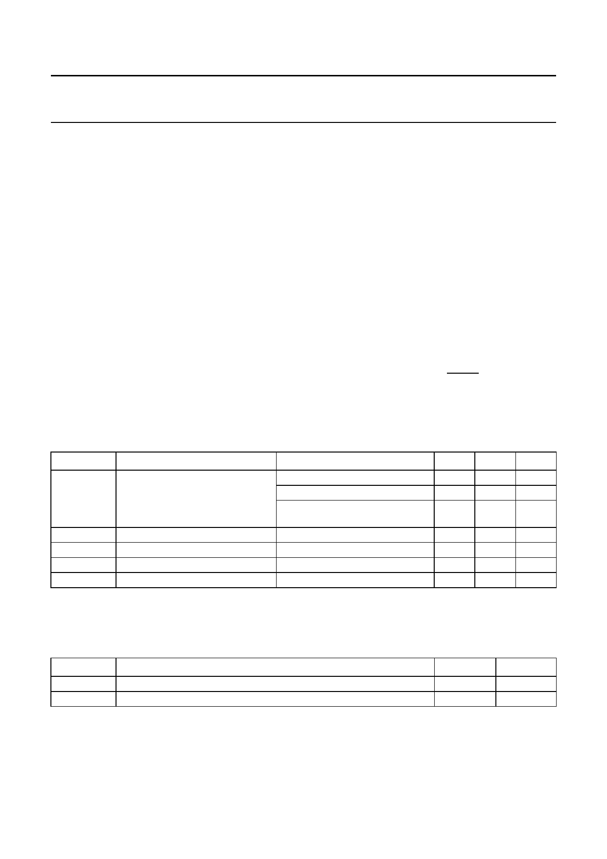
LIMITING VALUES
In accordance with the Absolute maximum System (IEC 134).
SYMBOL
VP1, VP2
PARAMETER
supply voltage
Ptot
total power dissipation
Tstg
storage temperature range
Tvj
virtual junction temperature
Vpr
reverse polarity
CONDITIONS
MIN.
operating
−
non-operating
−
load dump protected; during 50 ms; −
tr > 2.5 ms; note 1
Tcase < 30 °C
−
non-operating
−55
operating
−40
non-operating
−
Note
1. Regulator 1 operating, 0.5 mA ≤ IR1 ≤ 20 mA.
MAX.
18
30
50
15
150
150
6
UNIT
V
V
V
W
°C
°C
V
THERMAL CHARACTERISTICS
SYMBOL
Rth j-c
Rth j-amb
PARAMETER
thermal resistance from junction to case
thermal resistance from junction to ambient in free air
VALUE
8
40
UNIT
K/W
K/W
QUALITY SPECIFICATION
Quality according to UZW-BO/FQ-0601.
1995 Dec 13
5
Share Link: 