PI74FCT2827T Ver la hoja de datos (PDF) - Pericom Semiconductor
Número de pieza
componentes Descripción
Lista de partido
PI74FCT2827T Datasheet PDF : 5 Pages
| |||
PI74FCT827/828T
(25Ω Series) P174FCT2827/2828T
123456789012345678901234567890121234567890123456789012345678901212345678901234567890123456789012123456789012345678910102-3B45I67T89B012U12F34F56E78R90S12
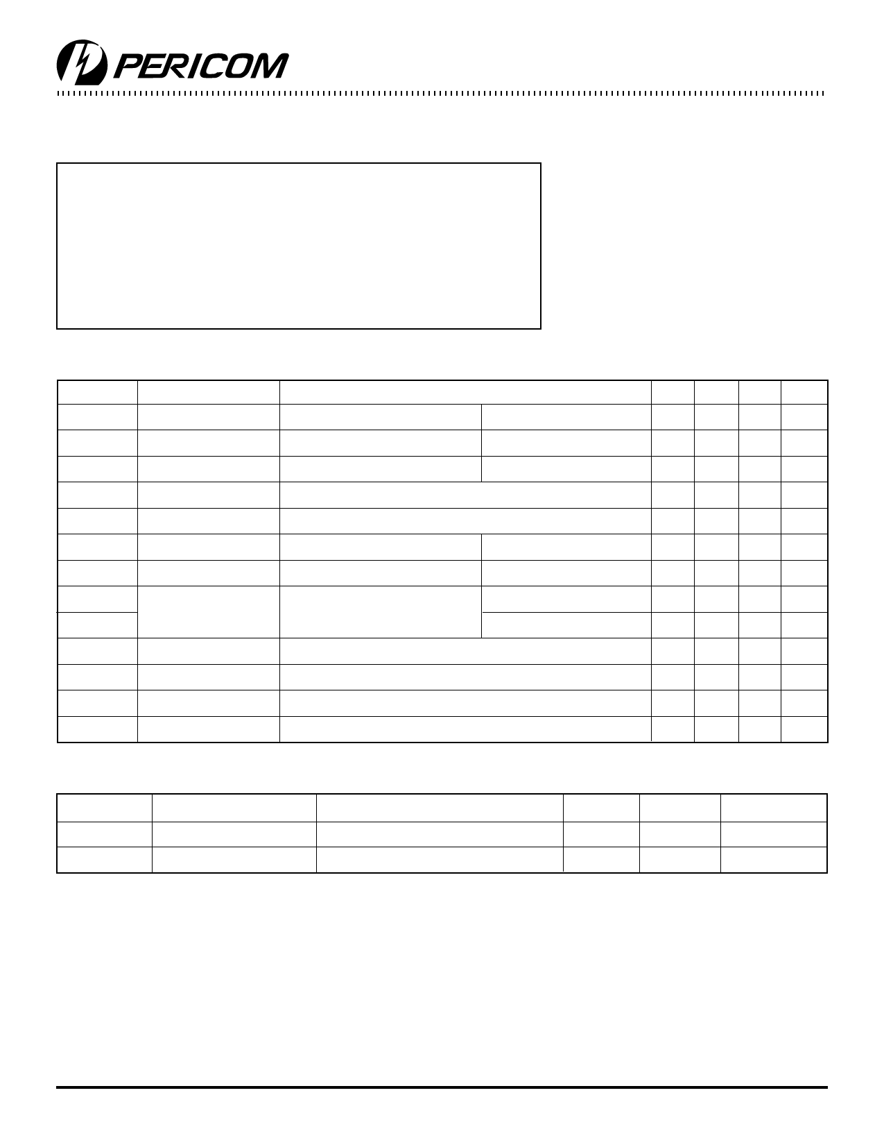
Maximum Ratings
(Above which the useful life may be impaired. For user guidelines, not tested.)
Storage Temperature ................................................................. –65°C to +150°C
Ambient Temperature with Power Applied .................................. -40°C to +85°C
Supply Voltage to Ground Potential (Inputs & Vcc Only) .......... –0.5V to +7.0V
Supply Voltage to Ground Potential (Outputs & D/O Only) ....... –0.5V to +7.0V
DC Input Voltage ......................................................................... –0.5V to +7.0V
DC Output Current .................................................................................... 120mA
Power Dissipation ......................................................................................... 0.5W
Note:
Stresses greater than those listed under
MAXIMUM RATINGS may cause permanent
damage to the device. This is a stress rating only
and functional operation of the device at these or
any other conditions above those indicated in
the operational sections of this specification is
not implied. Exposure to absolute maximum
rating conditions for extended periods may
affect reliability.
DC Electrical Characteristics (Over the Operating Range, TA = –40°C to +85°C, VCC = 5.0V ± 5%)
Parameters Description
Test Conditions(1)
Min. Typ(2) Max. Units
VOH
Output HIGH Voltage VCC = Min., VIN = VIH or VIL
IOH = –15.0mA
2.4 3.0
V
VOL
Output LOW Current VCC = Min., VIN = VIH or VIL
IOL = 48mA
0.3 0.50 V
VOL
Output LOW Current VCC = Min., VIN = VIH or VIL
IOL = 12mA (25Ω Series)
0.3 0.50 V
VIH
Input HIGH Voltage Guaranteed Logic HIGH Level
2.0
V
VIL
Input LOW Voltage Guaranteed Logic LOW Level
0.8 V
IIH
Input HIGH Current VCC = Max.
VIN = VCC
1 µA
IIL
Input LOW Current VCC = Max.
VIN = GND
–1 µA
IOZH
High Impedance
VCC = MAX.
VOUT = 2.7V
1 µA
IOZL
Output Current
VOUT = 0.5V
–1 µA
VIK
Clamp Diode Voltage VCC = Min., IIN = –18mA
–0.7 –1.2 V
IOFF
Power Down Disable VCC = GND, VOUT = 4.5V
— — 100 µA
IOS
Short Circuit Current VCC = Max.(3), VOUT = GND
–60 –120
mA
VH
Input Hysteresis
200
mV
Capacitance (TA = 25°C, f = 1 MHz)
Parameters(4) Description
CIN
Input Capacitance
COUT
Output Capacitance
Test Conditions
VIN = 0V
VOUT = 0V
Typ
Max.
Units
6
10
pF
8
12
pF
Notes:
1. For Max. or Min. conditions, use appropriate value specified under Electrical Characteristics for the applicable device type.
2. Typical values are at Vcc = 5.0V, +25°C ambient and maximum loading.
3. Not more than one output should be shorted at one time. Duration of the test should not exceed one second.
4. This parameter is determined by device characterization but is not production tested.
3
PS2029B 10/27/98
Share Link: 