DS2105S Ver la hoja de datos (PDF) - Dallas Semiconductor -> Maxim Integrated
Número de pieza
componentes Descripción
Lista de partido
DS2105S Datasheet PDF : 7 Pages
| |||
DS2105
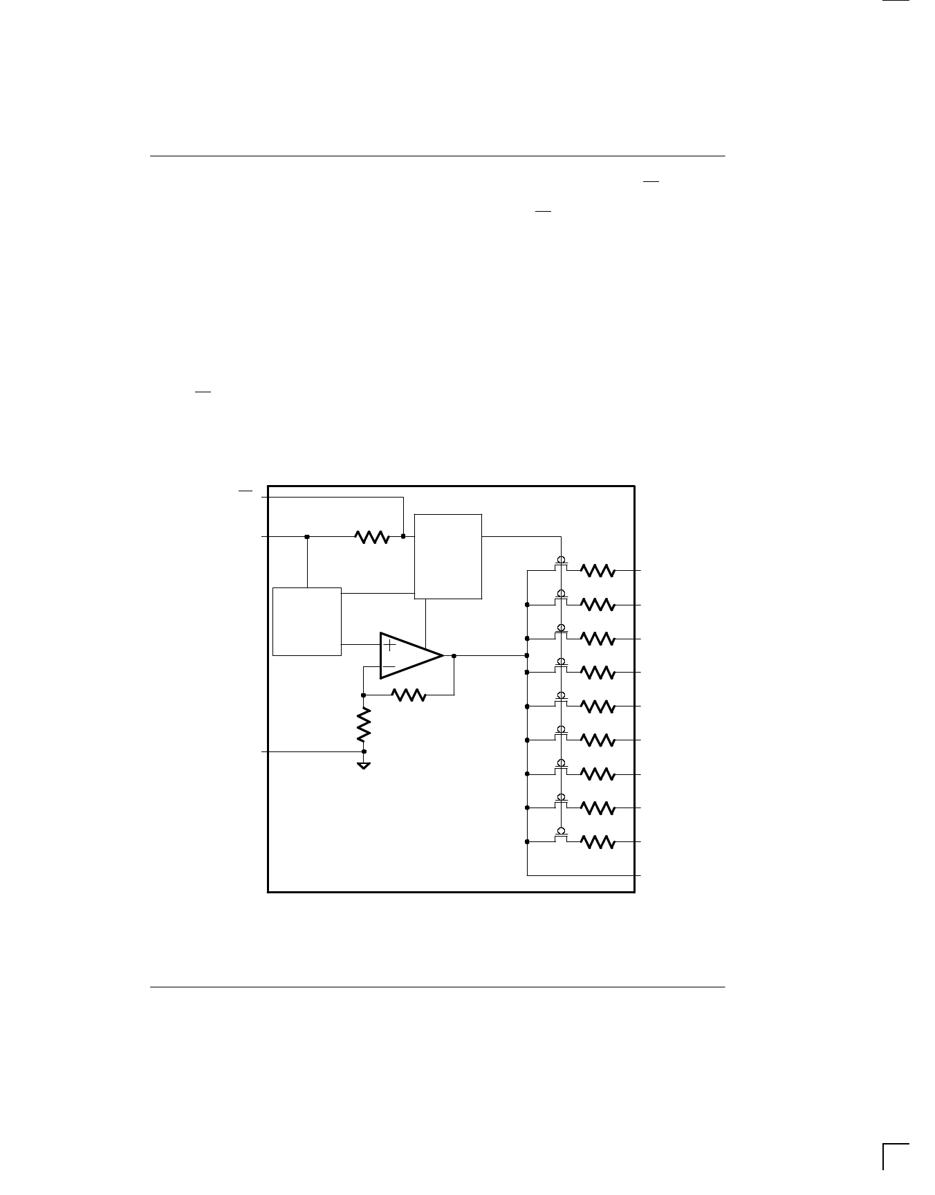
FUNCTIONAL DESCRIPTION
The DS2105 consists of a bandgap reference, buffer
amplifier, and nine termination resistors (Figure 1). The
bandgap reference circuit produces a precise 2.55V
level which is fed to a buffer amplifier. The buffer pro-
duces a 2.85V level and is capable of sourcing at least
24 mA into each of the termination resistors when the
signal line is low (active). When the driver for a given
signal line turns off, the terminator will pull the signal line
to 2.85V (quiescent state). To handle actively negated
SCSI signals, the buffer can sink 200 mA, and VREF will
move less than 60 mV. When all lines settle in the quies-
cent state, the regulator will consume about 5 mA.
When the DS2105 is put into power–down mode by
bringing PD low, the power–down circuitry will turn off
the transistors on each signal line. This will isolate the
DS2105 from the signal lines and effectively remove it
from the circuit. The power–down pin (PD) has an inter-
nal 50KΩ pull–up resistor. To place the DS2105 into an
active state, the PD pin should be left open circuited.
To ensure proper operation, both the TERMPWR1 and
TERMPWR2 pins must be connected to the SCSI bus
TERMPWR line and both the VREF1 and VREF2 pins
must be tied together externally. Each DS2105 requires
a 4.7 µF capacitor connected between the VREF pins
and ground. Figure 2 details a typical SCSI bus configu-
ration. In an 8–bit wide SCSI bus arrangement (“A”
Cable), two DS2105’s would be needed at each end of
the SCSI cable in order to terminate the 18 active signal
lines. In a 16–bit wide SCSI bus arrangement (“P”
Cable), three DS2105’s would be needed at each end of
the SCSI cable in order to terminate the 27 active signal
lines.
DS2105 BLOCK DIAGRAM Figure 1
PD
TERMPWR1
TERMPWR2
50K ohm
POWER
DOWN
CIRCUITRY
BANDGAP
REFERENCE
GND
110 ohms
R1
110 ohms
R2
110 ohms
R3
110 ohms
R4
110 ohms
R5
110 ohms
R6
110 ohms
R7
110 ohms
R8
110 ohms
R9
VREF1
VREF2
022698 2/7
Share Link: 