IDT7188L Ver la hoja de datos (PDF) - Integrated Device Technology
Número de pieza
componentes Descripción
Lista de partido
IDT7188L Datasheet PDF : 8 Pages
| |||
IDT7188S/L
CMOS Static RAM 64K (16K x 4-Bit)
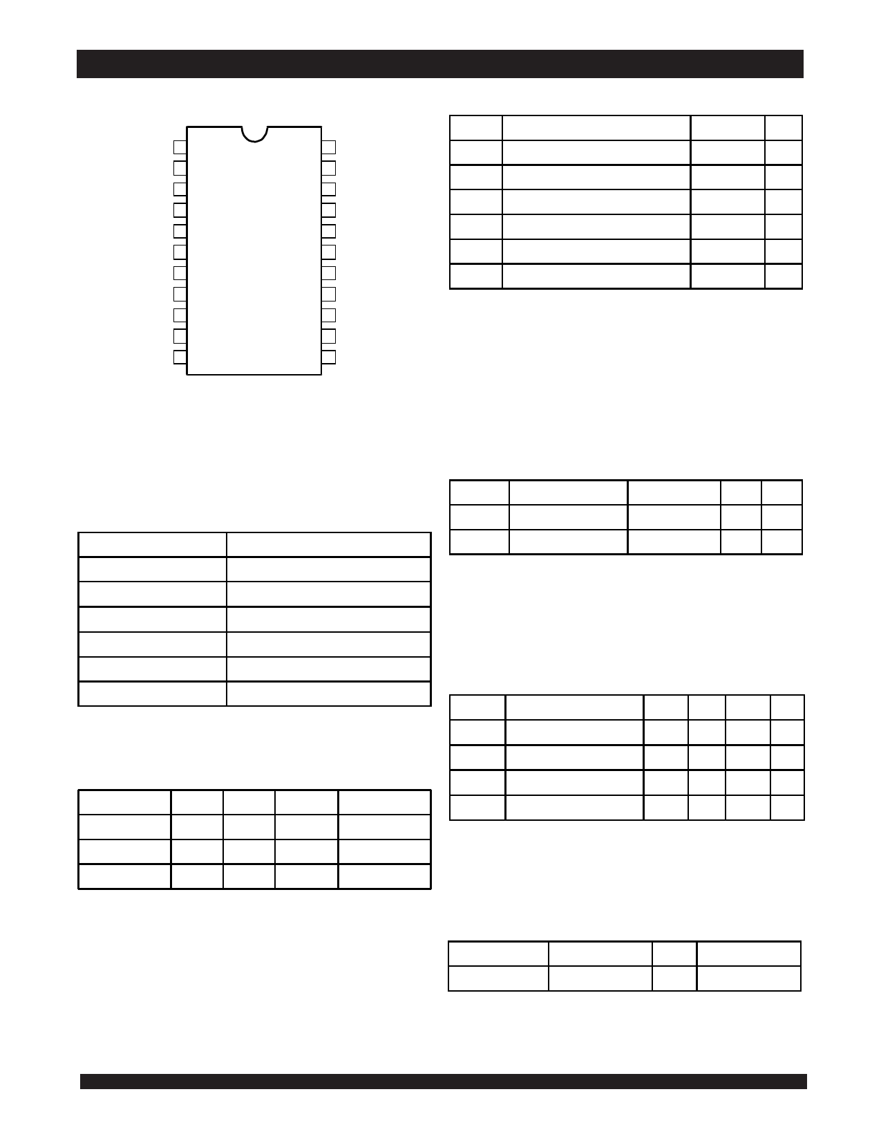
Pin Configuration
A0
A1
A2
A3
A4
A5
A6
A7
A8
CS
GND
1
22
2
21
3
20
4
19
5 D22-1 18
6
17
7
16
8
15
9
14
10
13
11
12
VCC
A13
A12
A11
A10
A9
I/O 3
I/O 2
I/O 1
I/O 0
WE ,
2989 drw 02
DIP
Top View
Pin Descriptions
Name
A0 - A13
CS
WE
I/O0 - I/O3
VCC
GND
Description
Address Inputs
Chip Select
Write Enable
Data Input/Output
Power
Ground
2989 tbl 01
Truth Table(1)
Mode
CS
WE
Standby
H
X
Read
L
H
Write
L
L
NOTE:
1. H = VIH, L = VIL, X = don't care.
I/O
High-Z
DOUT
DIN
Power
Standby
Active
Active
2989 tbl 02
Military Temperature Range
Absolute Maximum Ratings(1)
Symbol
Rating
Value
Unit
VTERM Terminal Voltage with Respect to GND -0.5 to +7.0 V
TA Operating Temperature
-55 to +125 oC
TBIAS Temperature Under Bias
-65 to +135 oC
TSTG Storage Temperature
-65 to +150 oC
PT Power Dissipation
1.0
W
IOUT DC Output Current
50
mA
NOTE:
2989 tbl 03
1. Stresses greater than those listed under ABSOLUTE MAXIMUM RATINGS
may cause permanent damage to the device. This is a stress rating only and
functional operation of the device at these or any other conditions above those
indicated in the operational sections of this specification is not implied. Exposure
to absolute maximum rating conditions for extended periods may affect
reliability.
Capacitance
(TA = +25°C, f = 1.0MHz, VCC = 0V)
Symbol
Parameter(1)
Conditions Max. Unit
CIN
Input Capacitance
VIN = 0V
6
pF
CI/O
I/O Capacitance
VOUT = 0V
6
pF
NOTE:
2989 tbl 04
1. This parameter is determined by device characterization, but is not production
tested.
Recommended DC Operating
Conditions
Symbol
Parameter
Min. Typ. Max. Unit
VCC Supply Voltage
4.5 5.0 5.5 V
GND Ground
0
0
0
V
VIH Input High Voltage
VIL Input Low Voltage
2.2
____
6.0
V
-0.5(1)
____
0.8
V
NOTE:
2989 tbl 05
1. VIL (min.) = –3.0V for pulse width less than 20ns,once per cycle.
Recommended Operating
Temperature and Supply Voltage
Grade
Temperature
GND
Vcc
Military
-55OC to +125OC 0V
5V ± 10%
2989 tbl 06
2
Share Link: 