MT9125AE Ver la hoja de datos (PDF) - Zarlink Semiconductor Inc
Número de pieza
componentes Descripción
Lista de partido
MT9125AE Datasheet PDF : 18 Pages
| |||
MT9125
Preliminary Information
configuration the ENB1 and ENB2 inputs are
ignored. If F0i is tied continuously to VSS, then SSI
operation will be assumed and the transcoder will
use the strobes connected to ENB1 and ENB2 as its
internal reference.
Power-Down Operation (PWRDN)
To minimize power consumption a pin selected,
power-down option is provided. Device power down
is accomplished by forcing the PWRDN pin to VSS.
This asynchronous control forces all internal clocking
to halt and the C2o, EN1, EN2, DSTo and ADPCMo
outputs to become tri-stated. Upon returning
PWRDN to VDD coincident with the next alignment
signal, all outputs will return to their active state and
the internal clocks are re-started. In this mode the
ADPCM algorithm is not reset to the 'optional reset
values', however, the self-convergent nature of the
algorithm will ensure that convergence of the
(AD)PCM streams will occur within 3496 frames as
specified by CCITT G.721.
Removal of the BCLK and MCLK inputs is not
necessary during power-down mode. If the device is
released from power-down without a valid MCLK the
ADPCMo and PCMo outputs will become active,
driving either continuous logic high or logic low, until
a MCLK signal is applied to resume internal
operation.
PWRDN is a schmidt trigger input.
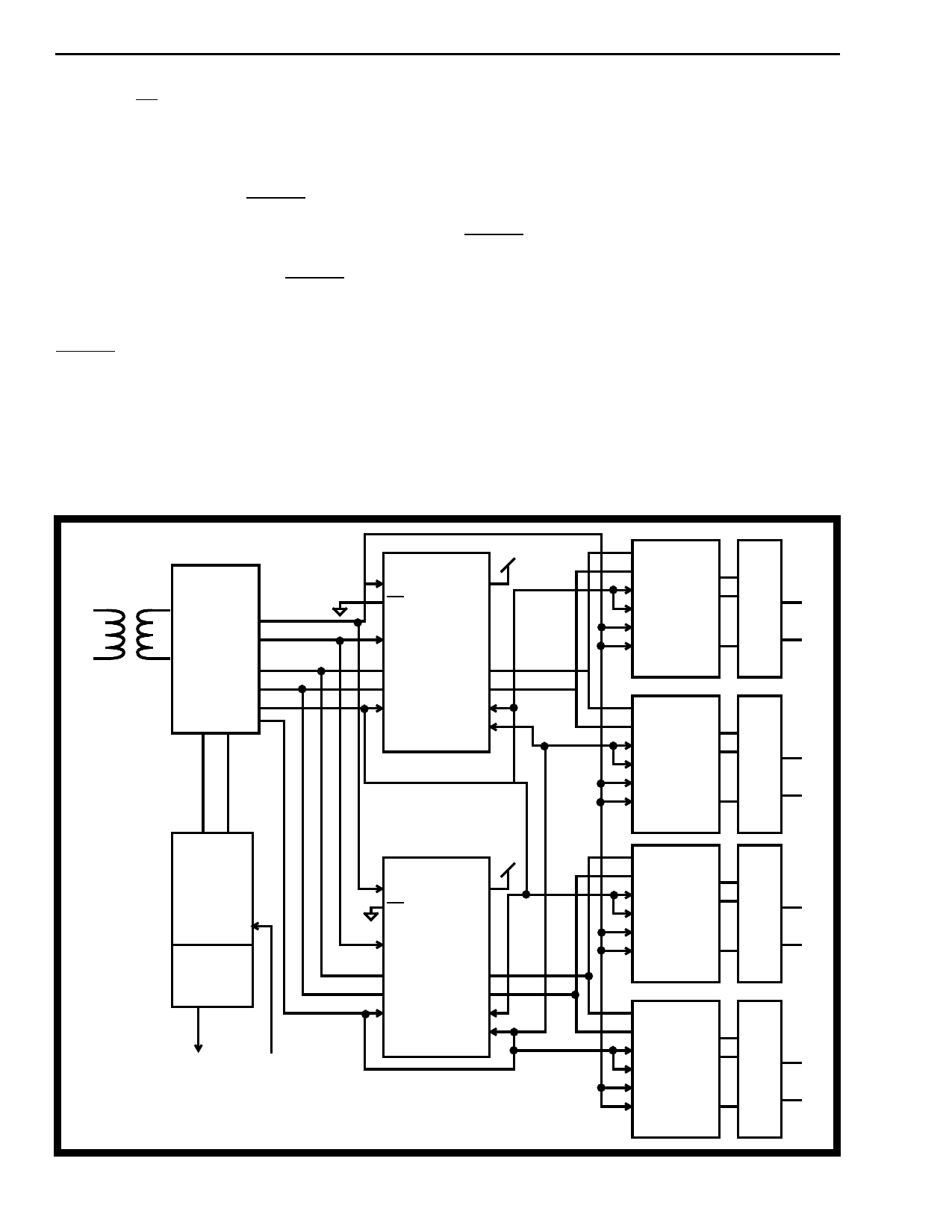
Applications
Various configurations of Pair Gain drops are
depicted in Figures 7, 8 and 9. These show
applications using mixed ST-BUS/SSI, all ST-BUS
and all SSI implementations. Figure10 shows an ST-
BUS line card application for Pair Gain while Figure
11 shows a 2-channel, wireless-set, base station
application based upon ST-BUS.
T
R
8-82
Lin+
Lin-
Lout+
Lout-
BCLK
MCLK
TX
RX
EN1
EN2
VDD
MT9125
BCLK
ENS
F0i
MCLK
ADPCMi
ADPCMo
ENA
DSTi
DSTo
ENB1
ENB2
Gate
Array
Ring
Generator
to SLICs
Hookswitch
from SLICs
VDD
MT9125
BCLK
ENS
F0i
MCLK
ADPCMi
ADPCMo
ENA
DSTi
DSTo
ENB1
ENB2
DX
DR
VFxL+
FSX
FSR
VFxL-
S
L
I
T
BCLKX
C
MCLKX VFRO
R
DX
DR
VFxL+
FSX
FSR
VFxL-
S
L
I
T
BCLKX
C
MCLKX VFRO
R
DX
DR
VFxL+
FSX
FSR
VFxL-
S
L
I
T
BCLKX
C
MCLKX VFRO
R
DX
DR
VFxL+
FSX
FSR
VFxL-
S
L
I
T
BCLKX
C
MCLKX VFRO
R
Figure 9 - Pair Gain Application (SSI/SSI)
Share Link: 