MD56V62160E Ver la hoja de datos (PDF) - LAPIS Semiconductor Co., Ltd.
Número de pieza
componentes Descripción
Lista de partido
MD56V62160E Datasheet PDF : 33 Pages
| |||

FEDD56V62160E-07
MD56V62160E
*Notes: 1. When CS is set “High” at a clock transition from “Low” to “High”, all inputs except CLK, CKE,
UDQM and LDQM are invalid.
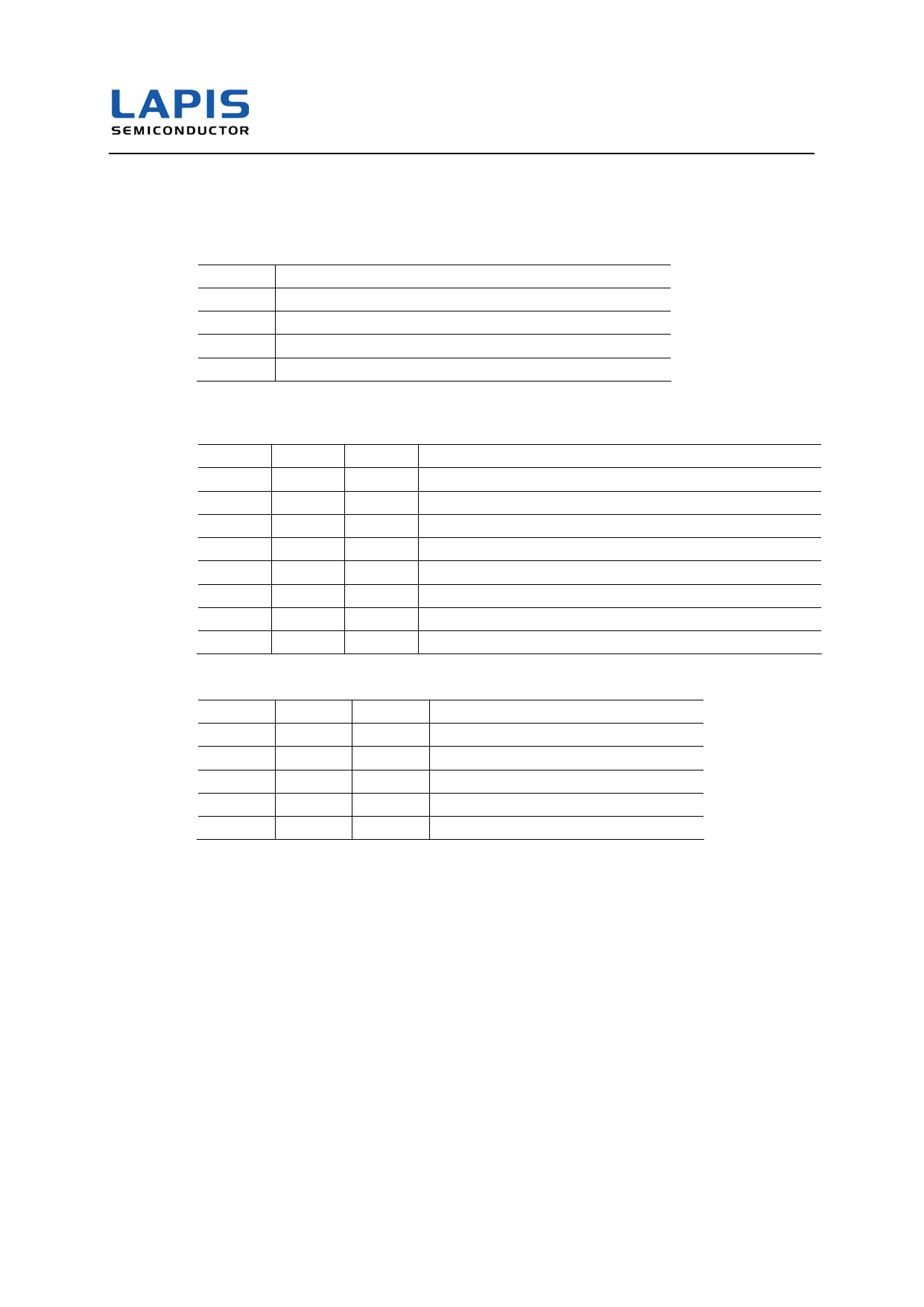
2. When issuing an active, read or write command, the bank is selected by A12 and A13.
A11
A12
0
0
0
1
1
0
1
1
Active, read or write
Bank A
Bank B
Bank C
Bank D
3. The auto precharge function is enabled or disabled by the A10 input when the read or write command
is issued.
A10
A12
A13
Operation
0
0
0
After the end of burst, bank A holds the idle status.
1
0
0
After the end of burst, bank A is precharged automatically.
0
0
1
After the end of burst, bank B holds the idle status.
1
0
1
After the end of burst, bank B is precharged automatically.
0
1
0
After the end of burst, bank C holds the idle status.
1
1
0
After the end of burst, bank C is precharged automatically.
0
1
1
After the end of burst, bank D holds the idle status.
1
1
1
After the end of burst, bank D is precharged automatically.
4. When issuing a precharge command, the bank to be precharged is selected by the A10 and A11 inputs.
A10
A12
A13
Operation
0
0
0
Bank A is precharged.
0
0
1
Bank B is precharged.
0
1
0
Bank C is precharged.
0
1
1
Bank D is precharged.
1
X
X
All banks are precharged.
5. The input data and the write command are latched by the same clock (Write latency = 0).
6. The output is forced to high impedance by (1CLK+ tOHZ ) after UDQM, LDQM entry.
11/33