EL7516IY Ver la hoja de datos (PDF) - Renesas Electronics
Número de pieza
componentes Descripción
Lista de partido
EL7516IY Datasheet PDF : 12 Pages
| |||
EL7516
During the second cycle, the power FET turns off and the
Schottky diode is forward biased, Figure 30. The energy
stored in the inductor is pumped to the output supplying
output current and charging the output capacitor. The
Schottky diode side of the inductor is clamp to a Schottky
diode above the output voltage, so the voltage drop across
the inductor is VIN - VOUT. The change in inductor current
during the second cycle is:
IL = t2 -V----I--N-----–---L-V-----O----U----T--
t2 = 1--f--S-–---W--D---
(EQ. 2)
For stable operation, the same amount of energy stored in
the inductor must be taken out. The change in inductor
current during the two cycles must be the same.
I1 + I2 = 0
-f-S--D--W---- -V---L-I--N-- + 1--f--S-–---W--D--- -V----I--N-----–---L-V-----O----U----T-- = 0
V----V-O---I-U-N---T-- = 1-----–-1----D---
(EQ. 3)
VIN
CIN
L
EL7516
D
VOUT
COUT
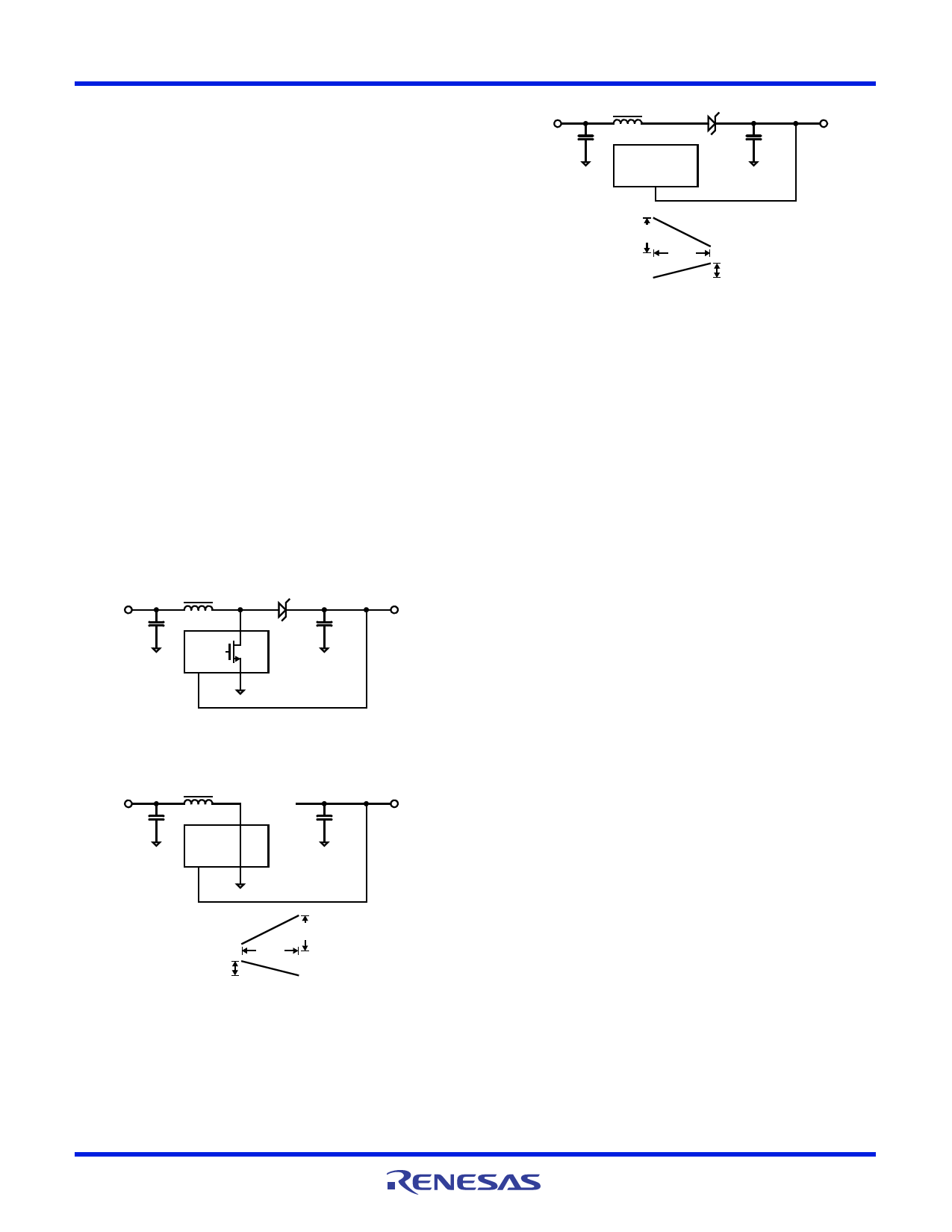
FIGURE 29. BOOST CONVERTER
VIN
CIN
L
EL7516
COUT
VOUT
IL
IL1
t1
VO
FIGURE 30. BOOST CONVERTER - CYCLE 1, POWER
SWITCH CLOSED
FN7333 Rev 6.00
October 9, 2007
VIN
CIN
L
D
EL7516
COUT
VOUT
IL2
IL
t2
VO
FIGURE 31. BOOST CONVERTER - CYCLE 2, POWER
SWITCH OPEN
Output Voltage
An external feedback resistor divider is required to divide the
output voltage down to the nominal 1.294V reference
voltage. The current drawn by the resistor network should be
limited to maintain the overall converter efficiency. The
maximum value of the resistor network is limited by the
feedback input bias current and the potential for noise being
coupled into the feedback pin. A resistor network less than
100k is recommended. The boost converter output voltage is
determined by the relationship:
VOUT
=
VFB
1
+
RR-----12-
(EQ. 4)
The nominal VFB voltage is 1.294V.
Inductor Selection
The inductor selection determines the output ripple voltage,
transient response, output current capability, and efficiency.
Its selection depends on the input voltage, output voltage,
switching frequency, and maximum output current. For most
applications, the inductance should be in the range of 2µH to
33µH. The inductor maximum DC current specification must
be greater than the peak inductor current required by the
regulator. The peak inductor current can be calculated:
ILPEAK = I--O-----U----T---V----I--N-V----O----U----T-- + 1 2 V--L---I--N-----V----O---V-U---O--T---U----T--F---–-R---V--E---I-NQ----- (EQ. 5)
Output Capacitor
Low ESR capacitors should be used to minimize the output
voltage ripple. Multilayer ceramic capacitors (X5R and X7R)
are preferred for the output capacitors because of their lower
ESR and small packages. Tantalum capacitors with higher
ESR can also be used. The output ripple can be calculated
as:
VO = -fI-S-O---W-U-----T------C---D-O--- + IOUT ESR
(EQ. 6)
For noise sensitive application, a 0.1µF placed in parallel
with the larger output capacitor is recommended to reduce
the switching noise coupled from the LX switching node.
Page 9 of 12
Share Link: 