PI74FCT3244 Ver la hoja de datos (PDF) - Pericom Semiconductor
Número de pieza
componentes Descripción
Lista de partido
PI74FCT3244 Datasheet PDF : 7 Pages
| |||
PI74FCT3244
3.3V 8-Bit Buffer/Line Driver
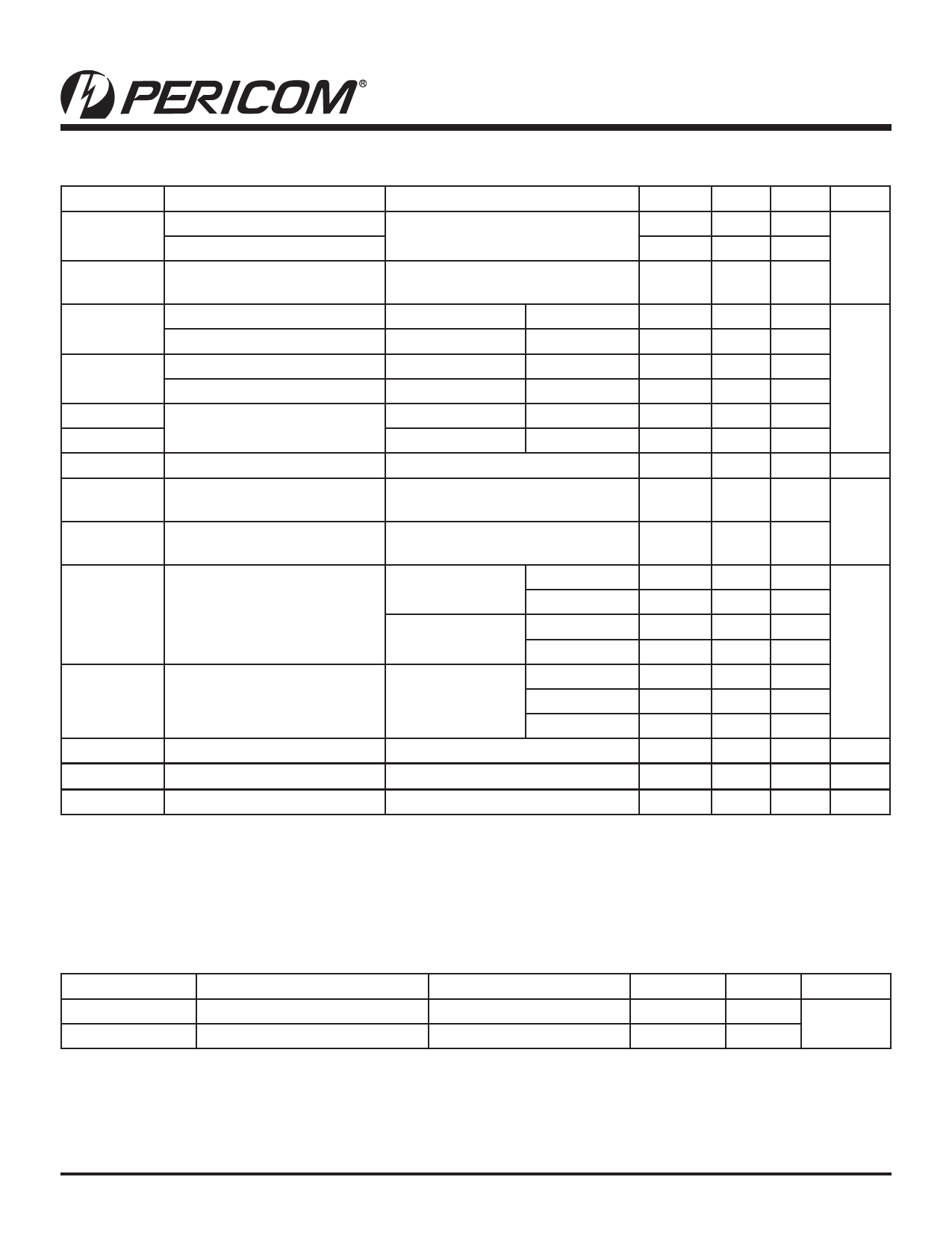
DC Electrical Characteristics (TA = –40°C to +85°C, VCC = 2.7V to 3.6V)
Parameters
Description
Test Conditions(1)
Min. Typ.(2) Max.
Input HIGH Voltage (Input pins)
2.2
5.5
VIH
Guaranteed Logic HIGH Level
Input HIGH Voltage (I/O pins)
2.0
5.5
VIL
Input LOW Voltage
(Input and I/O pins)
Guaranteed Logic LOW Level
–0.5
0.8
IIH
Input HIGH Current (Input pins) VCC = Max.
Input HIGH Current (I/O pins) VCC = Max.
VIN = 5.5V
VIN = VCC
±1
±1
IIL
Input LOW Current (Input pins) VCC = Max.
Input LOW Current (I/O pins) VCC = Max.
VIN = GND
VIN = GND
±1
±1
IOZH
High Impedance Output Current VCC = Max.
VOUT = 5.5V
±1
IOZL
(3-State Output pins)
VCC = Max.
VOUT = GND
±1
VIK
Clamp Diode Voltage
VCC = Min., IIN = –18mA
–0.7 –1.2
IODH
Output HIGH Current
VCC = 3.3V, VIN = VIH or VIL,
VO = 1.5V(3)
–36
–60 –110
IODL
Output LOW Current
VCC = 3.3V, VIN = VIH or VIL,
VO = 1.5V(3)
50
90
200
VOH
Output HIGH Voltage
VCC = Min.,
IOH = –0.1mA VCC-0.2
VIN = VIH or VIL IOH = –3mA
2.4
3.0
VCC = 3.0V,
IOH = –8mA
2.4(5)
3.0
VIN = VIH or VIL IOH = –24mA
2.0
VOL
Output LOW Voltage
IOS
Short Circuit Current(4)
VCC = Min.,
VIN = VIH or VIL
IOL = 0.1mA
IOL = 16mA
IOL = 24mA
VCC = Max.(3), VOUT = GND
0.2
0.2 0.4
0.3 0.5
–60
–85 –240
IOFF
Power Down Disable
VCC = 0V, VIN or VOUT ≤ 4.5V
±100
VH
Input Hysteresis
150
Notes:
1. For Max. or Min. conditions, use appropriate value specified under Electrical Characteristics for the applicable device type.
2. Typical values are at Vcc = 3.3V, +25°C ambient and maximum loading.
3. Not more than one output should be shorted at one time. Duration of the test should not exceed one second.
4. This parameter is guaranteed but not tested.
5. VOH = VCC – 0.6V at rated current.
Units
V
µA
V
mA
V
mA
µA
mV
Capacitance (TA = 25°C, f = 1 MHz)
Parameters(1)
Description
CIN
Input Capacitance
COUT
Output Capacitance
Notes:
1. Determined by device characterization.
Test Conditions
VIN = 0V
VOUT = 0V
Typ.
4.5
5.5
Max.
6
8
Units
pF
06-0218
3
PS7067I
06/20/06
Share Link: 