ML9473TB Ver la hoja de datos (PDF) - LAPIS Semiconductor Co., Ltd.
Número de pieza
componentes Descripción
Lista de partido
ML9473TB Datasheet PDF : 20 Pages
| |||
LAPIS Semiconductor
FEDL9473-01
ML9473
FUNCTIONAL DESCRIPTION
Operation
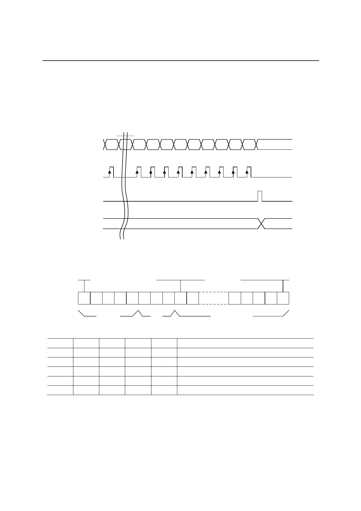
As shown in “Data Structure”, the display data consists of the data field corresponding to the output for turning
the segments on or off and the select field that selects field that selects the input block of data. Data input to the
DATA_IN pin is loaded into the 68-bit shift register, transferred to the 60-bit latch while the load signal is at “H”
level, and then output via the 60-dot segment driver.
D1
DATA_IN
D60 DM1 DM2 DM3 C1 C2 C3 C4 C5
1
CLOCK
60 61 62 63 64 65 66 67 68
LOAD
Data in
display
latch
Data Structure
Input data
End bit
Old data
Corresponds to SEG1
New data
First bit
Corresponds to SEG60
C5
C4
C3
C2
C1 DM3 DM2 DM1 D60 D59
D5
D4
D3
D2
D1
Select bit
(5 bits)
Dummy bit
(3 bits)
LCD display data
(60 bits)
Correspondence between select bits and COM1 to COM5
C5
C4
C3
C2
C1
Description
0
0
0
0
1
Display data corresponding to COM1
0
0
0
1
0
Display data corresponding to COM2
0
0
1
0
0
Display data corresponding to COM3
0
1
0
0
0
Display data corresponding to COM4
1
Notes: 1.
2.
0
0
0
0
Display data corresponding to COM5
Arbitrary data can be set for the dummy bits.
Select bit, C1 to C5, selects 60-bit latches that correspond to COM1 to COM5, respectively.
Therefore, if “1” is set for more than one select bit, data is set to all the corresponding 60-bit latches.
Example:
If “1” is set to all the select bits C1 to C5, the display data of D1 to D60 is set to all the 60-bit latches that
correspond to COM1 to COM5.
9/20
Share Link: 