HD74HC75P Ver la hoja de datos (PDF) - Renesas Electronics
Número de pieza
componentes Descripción
Lista de partido
HD74HC75P Datasheet PDF : 8 Pages
| |||
HD74HC75
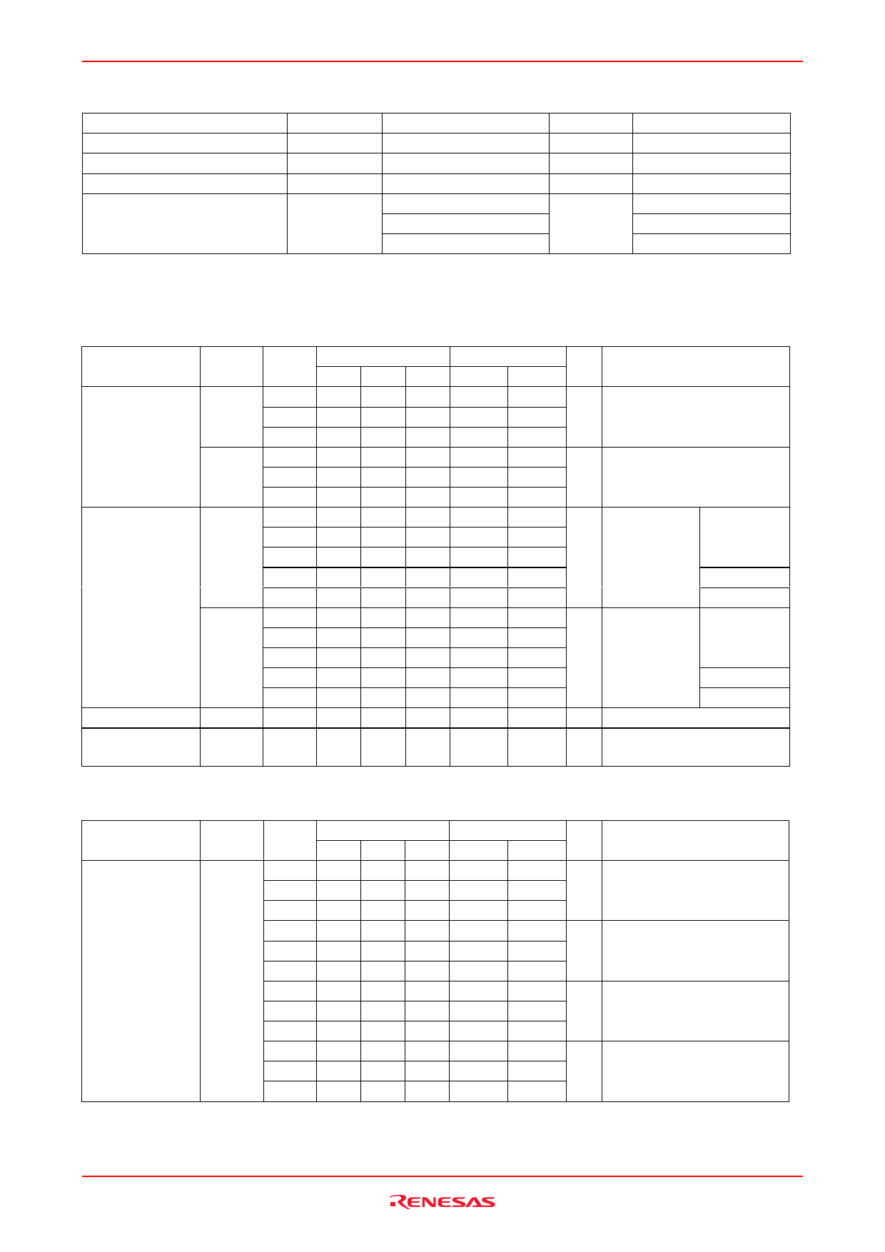
Recommended Operating Conditions
Item
Symbol
Ratings
Supply voltage
Input / Output voltage
VCC
VIN, VOUT
2 to 6
0 to VCC
Operating temperature
Ta
–40 to 85
Input rise / fall time*1
0 to 1000
tr, tf
0 to 500
0 to 400
Note: 1. This item guarantees maximum limit when one input switches.
Waveform: Refer to test circuit of switching characteristics.
Unit
V
V
°C
ns
Conditions
VCC = 2.0 V
VCC = 4.5 V
VCC = 6.0 V
Electrical Characteristics
Item
Input voltage
Output voltage
Input current
Quiescent supply
current
Symbol
VIH
VIL
VOH
VOL
Iin
ICC
VCC (V)
2.0
4.5
6.0
2.0
4.5
6.0
2.0
4.5
6.0
4.5
6.0
2.0
4.5
6.0
4.5
6.0
6.0
6.0
Ta = 25°C
Min Typ Max
1.5 — —
3.15 — —
4.2 — —
— — 0.5
— — 1.35
— — 1.8
1.9 2.0 —
4.4 4.5 —
5.9 6.0 —
4.18 — —
5.68 — —
— 0.0 0.1
— 0.0 0.1
— 0.0 0.1
— — 0.26
— — 0.26
— — ±0.1
— — 2.0
Ta = –40 to+85°C
Min Max Unit
Test Conditions
1.5
—
V
3.15
—
4.2
—
—
0.5 V
—
1.35
—
1.8
1.9
—
V Vin = VIH or VIL IOH = –20 µA
4.4
—
5.9
—
4.13
—
IOH = –4 mA
5.63
—
IOH = –5.2 mA
—
0.1
V Vin = VIH or VIL IOL = 20 µA
—
0.1
—
0.1
—
0.33
IOL = 4 mA
—
0.33
IOL = 5.2 mA
—
±1.0 µA Vin = VCC or GND
—
20 µA Vin = VCC or GND, Iout = 0 µA
Switching Characteristics (CL = 50 pF, Input tr = tf = 6 ns)
Item
Propagation delay
time
Symbol VCC (V)
tPLH, tPHL 2.0
4.5
6.0
2.0
4.5
6.0
2.0
4.5
6.0
2.0
4.5
6.0
Ta = 25°C
Ta = –40 to +85°C
Min Typ Max Min Max Unit
Test Conditions
— — 125 —
155 ns Data to Q
— 12 25
—
31
— — 21
—
26
— — 110 —
140 ns Data to Q
— 13 22
—
28
— — 19
—
24
— — 145 —
180 ns Latch Enable to Q
— 12 29
—
36
— — 25
—
31
— — 125 —
155 ns Latch Enable to Q
— 13 25
—
31
— — 21
—
26
Rev.2.00, Oct 06, 2005 page 3 of 7
Share Link: 