HD74LVC74 Ver la hoja de datos (PDF) - Renesas Electronics
Número de pieza
componentes Descripción
Lista de partido
HD74LVC74 Datasheet PDF : 7 Pages
| |||
HD74LVC74
Switching Characteristics
Item
Maximum clock frequency
Propagation delay time
Setup time
Hold time
Pulse width
Recovery time
Input capacitance
Output capacitance
Symbol
fmax
tPLH
tPHL
tPLH
tPHL
tsu
th
tw
trec
CIN
CO
VCC (V)
2.7
3.3±0.3
5.0±0.5
2.7
3.3±0.3
5.0±0.5
2.7
3.3±0.3
5.0±0.5
2.7
3.3±0.3
5.0±0.5
2.7
3.3±0.3
5.0±0.5
2.7
3.3±0.3
5.0±0.5
2.7
3.3±0.3
5.0±0.5
2.7
3.3±0.3
5.0±0.5
2.7
2.7
Ta = –40 to 85°C
Min
Typ
Max
150.0 —
—
150.0 —
—
150.0 —
—
—
6.0
9.0
1.5
5.0
8.0
—
4.0
6.5
—
6.5
9.0
1.5
5.0
8.0
—
4.0
6.5
4.0
—
—
3.0
—
—
3.0
—
—
2.0
—
—
2.0
—
—
2.0
—
—
4.0
—
—
4.0
—
—
4.0
—
—
6.0
—
—
5.0
—
—
4.0
—
—
3.0
—
—
2.0
—
—
2.0
—
—
—
3.0
—
—
15.0
—
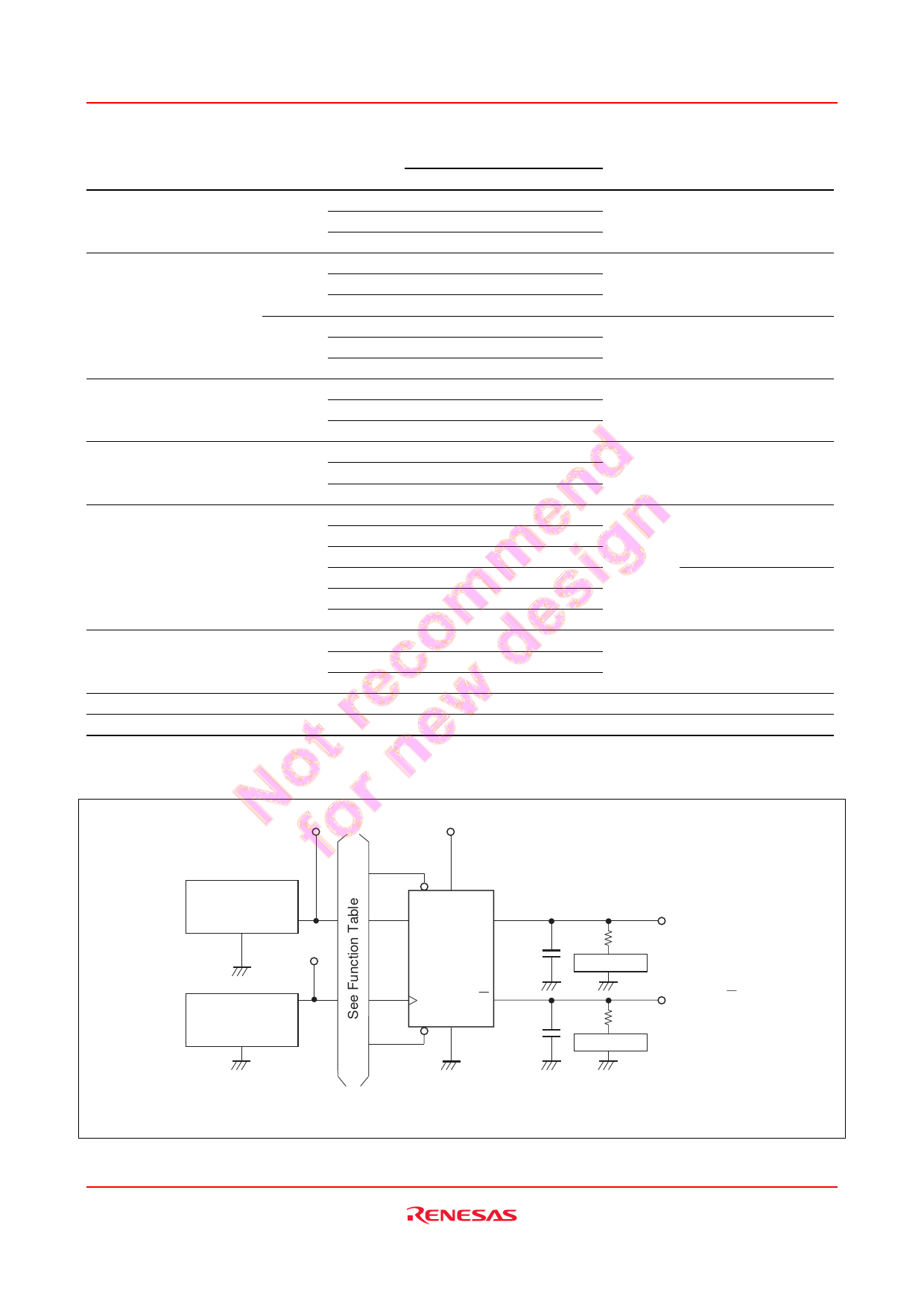
Test Circuit
Input
VCC
Unit
MHz
ns
ns
ns
ns
ns
ns
pF
pF
From
(Input)
To
(Output)
CLK
Q, Q
PR or CLR Q, Q
CK
PR or CLR
Pulse Generator
Zout = 50 Ω
Input
Pulse Generator
Zout = 50 Ω
PR
D
CK
CLR
Q
CL =
50 pF
Q
CL =
50 pF
450 Ω
50 Ω Scope
Output Q
450 Ω
50 Ω Scope
Output Q
Notes: 1. CL includes probe and jig capacitance.
2. Test is put into the each flip flops.
Rev.4.00 Jul. 22, 2004 page 4 of 6
Share Link: 