HD74LVCZ244A Ver la hoja de datos (PDF) - Renesas Electronics
Número de pieza
componentes Descripción
Lista de partido
HD74LVCZ244A Datasheet PDF : 9 Pages
| |||
HD74LVCZ244A
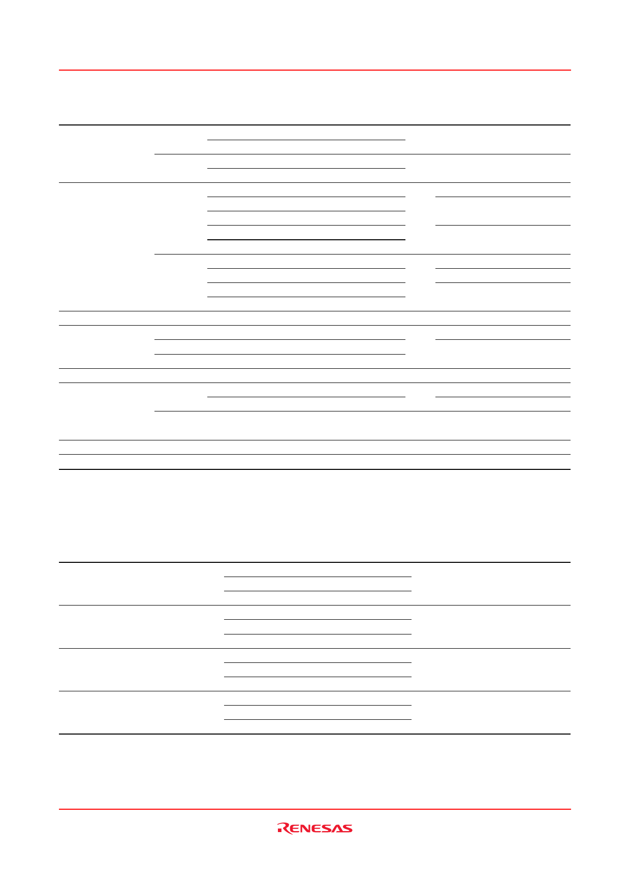
Electrical Characteristics
Item
Input voltage
Output voltage
Symbol
VIH
VIL
VOH
VOL
Input current
Off state output
current
Output leak current
Quiescent supply
current
IIN
IOZ
IOZPU
IOZPD
IOFF
ICC
∆ICC
VCC (V)
2.7 to 3.6
4.5 to 5.5
2.7 to 3.6
4.5 to 5.5
2.7 to 5.5
2.7
3.0
3.0
4.5
2.7 to 5.5
2.7
3.0
4.5
0 to 5.5
2.7 to 5.5
0 to 1.5
1.5 to 0
0
2.7 to 3.6
2.7 to 5.5
2.7 to 3.6
Min
Typ
2.0
—
VCC×0.7 —
—
—
—
—
VCC–0.2 —
2.2
—
2.4
—
2.2
—
3.8
—
—
—
—
—
—
—
—
—
—
—
—
—
—
—
—
—
—
—
—
—
—
—
—
—
Input capacitance CIN
3.3
—
3.4
Output capacitance CO
3.3
—
7.5
Note: 1. This applies in the disabled state only.
Max
—
—
0.8
VCC×0.3
—
—
—
—
—
0.2
0.4
0.55
0.55
±5
±5
±5
±5
±5
225
350
500
—
—
Unit
V
V
V
V
µA
µA
µA
µA
µA
pF
pF
(Ta = –40 to 85°C)
Test Conditions
IOH = –100 µA
IOH = –12 mA
IOH = –24 mA
IOL = 100 µA
IOL = 12 mA
IOL = 24 mA
VIN = 0 to 5.5 V
VOUT = 0 to 5.5 V
VOUT = 0.5 to 5.5 V,
Output enable = don’t care
VIN or VO = 5.5 V
VIN = 3.6 to 5.5 V *1, IO = 0
VIN = VCC or GND
VIN = one input at (VCC–0.6) V,
other inputs at VCC or GND
VIN = VCC or GND
VOUT = VCC or GND
Switching Characteristics
Item
Symbol VCC (V) Min
Typ
Propagation delay time tPLH
2.7
—
—
tPHL
3.3±0.3 1.5
—
5.0±0.5 —
—
Output enable time
tZH
2.7
—
—
tZL
3.3±0.3 1.5
—
5.0±0.5 —
—
Output disable time
tHZ
2.7
—
—
tLZ
3.3±0.3 1.5
—
5.0±0.5 —
—
Between output pin skew *1 tOSLH
2.7
—
—
tOSHL
3.3±0.3 —
—
5.0±0.5 —
—
Note: 1. This parameter is characterized but not tested.
tOSLH = |tPLHm–tPLHn|, tOSHL = |tPHLm–tPHLn|
Max
6.9
5.9
4.5
8.6
7.6
6.1
6.8
6.5
5.5
—
1.0
1.0
Unit
ns
ns
ns
ns
(Ta = –40 to 85°C)
FROM
TO
(Input) (Output)
A
Y
G
Y
G
Y
Rev.3.00 Aug. 18, 2004 page 4 of 8
Share Link: 