HD74LVC244AFPEL Ver la hoja de datos (PDF) - Renesas Electronics
Número de pieza
componentes Descripción
Lista de partido
HD74LVC244AFPEL Datasheet PDF : 7 Pages
| |||
HD74LVC244A
Switching Characteristics
Ta = –40 to 85°C
Item
Symbol VCC (V) Min
Typ
Max
Propagation delay time
tPLH
2.7
—
—
7.5
tPHL
3.3±0.3 1.5
—
6.5
5.0±0.5 —
—
5.0
Output enable time
tZH
2.7
—
—
9.0
tZL
3.3±0.3 1.5
—
8.0
5.0±0.5 —
—
6.5
Output disable time
tZH
2.7
—
—
8.0
tLZ
3.3±0.3 1.5
—
7.0
5.0±0.5 —
—
6.0
Between output pins skew tOSLH
2.7
—
—
—
*1
tOSHL
3.3±0.3 —
—
1.0
5.0±0.5 —
—
1.0
Input capacitance
CIN
2.7
—
3.0
—
Output capacitance
CO
2.7
—
15.0
—
Note: 1. This parameter is characterized but not tested.
tosLH = | tPLHm - tPLHn|, tosHL = | tPHLm - tPHLn|
Unit
ns
ns
ns
ns
pF
pF
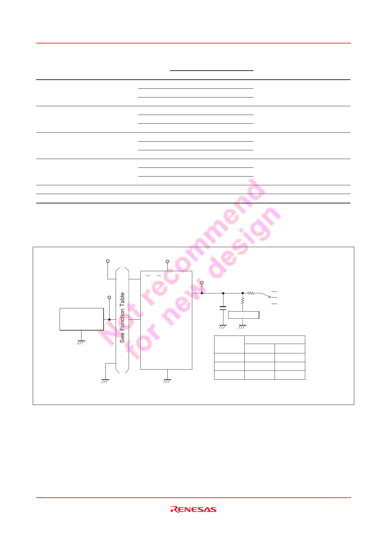
Test Circuit
VCC
VCC
From
(Input)
A
To
(Output)
Y
G
Y
G
Y
Input
Pulse generator
Zout = 50 Ω
1G, 2G
1Y1 to 2Y4
1A1 to 2A4
Output
CL =
50 pF
500 Ω S1
450 Ω
50 Ω Scope
OPEN
*1 See under table
GND
Symbol
tPLH / t PHL
tZH/ t HZ
tZL / t LZ
S1
Vcc=2.7V,
3.3±0.3V
Vcc=5.0±0.5V
OPEN OPEN
GND
GND
6V
2×Vcc
Note: 1. CL includes probe and jig capacitance.
Rev.4.00 Jul. 27, 2004 page 4 of 6
Share Link: 