HD74HC292P Ver la hoja de datos (PDF) - Renesas Electronics
Número de pieza
componentes Descripción
Lista de partido
HD74HC292P Datasheet PDF : 10 Pages
| |||
HD74HC292/HD74HC294
Programmable Frequency Divider/Digital Timer
REJ03D0608–0200
(Previous ADE-205-486)
Rev.2.00
Jan 31, 2006
Description
This device divides the incoming clock frequency by a number (a power of 2) that is preset by the Programming inputs.
It has two Clock inputs, either of which may be used as a clock inhibit. The device also has an active-low Reset, which
initializes the internal flip-flop states. Test Point outputs (TP1, TP2, TP3) are provided with HD74HC292 to facilitate
incoming inspections.
Test Point output is provided with HD74HC294 to facilitate incoming inspections.
Features
• High Speed Operation: tpd (Clock to Q) = 16 ns typ (CL = 50 pF)
• High Output Current: Fanout of 10 LSTTL Loads
• Wide Operating Voltage: VCC = 2 to 6 V
• Low Input Current: 1 µA max
• Low Quiescent Supply Current: ICC (static) = 4 µA max (Ta = 25°C)
• Ordering Information
Part Name
Package Type
Package Code
(Previous Code)
Package
Abbreviation
HD74HC292P
DILP-16 pin
PRDP0016AE-B
(DP-16FV)
P
HD74HC294FPEL SOP-16 pin (JEITA)
PRSP0016DH-B
(FP-16DAV)
FP
Note: Please consult the sales office for the above package availability.
Taping Abbreviation
(Quantity)
—
EL (2,000 pcs/reel)
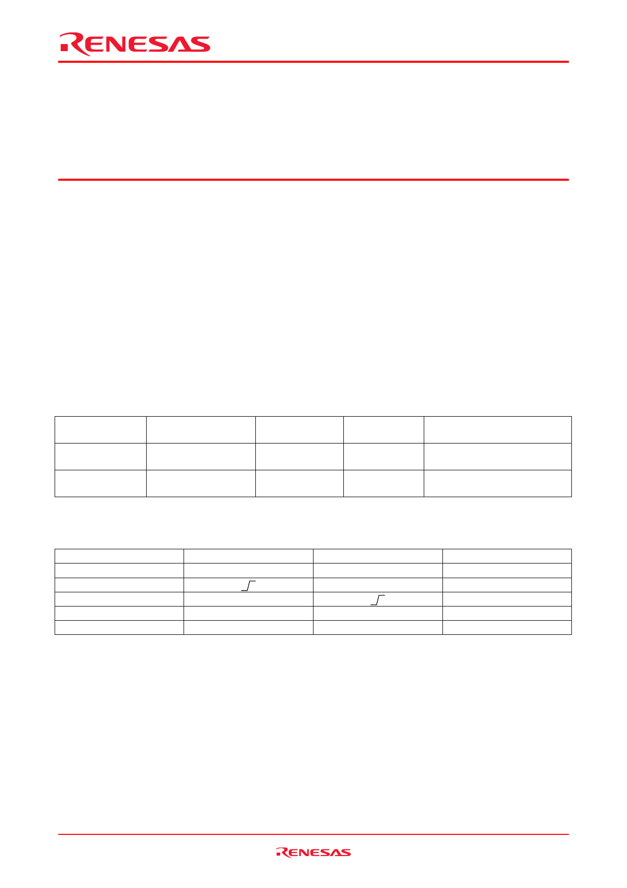
Function Table
CLR
L
H
H
H
H
H : high level
L : low level
CLK1
X
L
H
X
CLK2
X
L
X
H
Q Output Mode
Cleared to L
Count
Count
Inhibit
Inhibit
Rev.2.00 Jan 31, 2006 page 1 of 9
Share Link: 