LA5693D Ver la hoja de datos (PDF) - SANYO -> Panasonic
Número de pieza
componentes Descripción
Lista de partido
LA5693D Datasheet PDF : 7 Pages
| |||
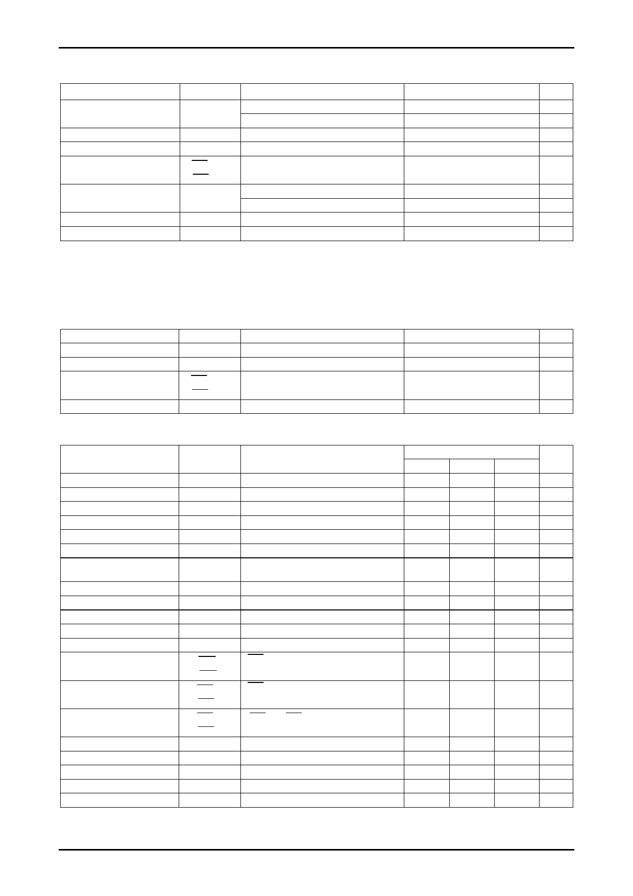
Specifications
Maximum Ratings at Ta = 25°C
LA5693D, LA5693MD
Parameter
Control pin voltage
Symbol
VCONT max 1s
Conditions
Ratings
Unit
60
V
41
V
Control pin current
CK input voltage
Reset pin voltage
Allowable power dissipation
ICONT max
VCK max
V RES(1) max,
V RES(2) max
Pd max
LA5693D
11 mA
25
V
41
V
500 mW
LA5693MD
350 mW
Operating temperature
Topr
-40 to +85 °C
Storage temperature
Tstg
-55 to +150 °C
* : A PNP transistor is connected to the LA5693D, LA5693M externally to provide a low-saturation voltage regulator.
Therefore, ICONT≈100mA will flow, as starting current, in the VCC range where the output cannot be regulated.
Caution 1) Absolute maximum ratings represent the value which cannot be exceeded for any length of time.
Caution 2) Even when the device is used within the range of absolute maximum ratings, as a result of continuous usage under high temperature, high current,
high voltage, or drastic temperature change, the reliability of the IC may be degraded. Please contact us for the further details.
Operating Conditions at Ta = 25°C
Parameter
Control pin voltage
Control pin current
Reset output current
Reset detection voltage
Symbol
VCONT
ICONT max
V RES(1) max,
V RES(2) max
VS min
Conditions
External R pull-up
Ratings
Unit
6 to 40
V
10 mA
8 mA
4
V
Electrical Characteristics at Ta = 25°C, VCC = 14V, IO=50mA, unless otherwise specified.
Parameter
Symbol
Conditions
Ratings
min
typ
Output voltage
VO
4.8
5.0
Line regulation1
ΔVOLN1
9V ≤ VCC ≤ 16V
2
Line regulation2
ΔVOLN2
6V ≤ VCC ≤ 40V
4
Load regulation
ΔVOLD
1mA ≤ IO ≤ 50mA
4
Current dissipation
ICC
IO=0
4.4
Output noise voltage
Temperature coefficient of
output voltage
Reference voltage
‘H’-level CK input voltage
‘L’-level CK input voltage
‘H’-level CK input current
‘L’-level CK input current
‘H’-level reset output voltage
‘L’-level reset output voltage 1
VNO
∆VO/ΔTa
VREF
VIH
VIL
IIH
IIL
V ORH(1)/
V ORH(2)
V ORL(1)1/
V ORL(2)1
10Hz ≤ f ≤ 100kHz, VCK = 0V
IO = 5mA, –40°C ≤ Ta ≤ +85°C
VCK = 5V
VCK = 0V
RES(2): 10kΩ pull-up
RES(2): 10kΩ pull-up
150
±0.2
1.13
1.18
2
0.3
-1.0
-0.1
4.8
5.0
40
‘L’-level reset output voltage 2
V ORL(1)2/
I RES(1) = I RES(2) = 8mA
0.16
V ORL(2)2
CK input pulse width
Reset output delay time
Watchdog time
Watchdog reset time
Reset hysteresis voltage
tCKW
td
tWD
tWR
Vhys
VCK = 5V
Ct = 1μF
Ct = 1μF
Ct = 1μF
VS = 4.5V
3
7.5
10
30
40
0.1
0.25
100
200
max
5.2
5
30
30
6.5
Unit
V
mV
mV
mV
mA
μV
mV/°C
1.23
V
V
0.8
V
0.7 mA
μA
5.2
V
200 mV
0.8
V
μs
12.5 ms
50 ms
0.4 ms
300 mV
No.A2085-2/7
Share Link: 