RF2461PCBA Ver la hoja de datos (PDF) - RF Micro Devices
Número de pieza
componentes Descripción
Lista de partido
RF2461PCBA Datasheet PDF : 14 Pages
| |||
RF2461
Preliminary
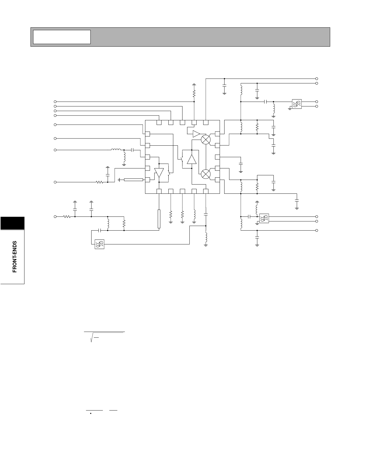
Application Schematic
NOTE:
Microstrip Inductor, Z0 = 50 Ω, L = 102 mils
suggested compared values.
LO IN
ENABLE
IP SET
IF SEL
LNA GAIN
MIX GAIN
LNA IN
VCC1
1
4.3 nH
2
33 nF
16 nH
3
100 pF
51 Ω
4
50 Ω µstrip
5
L=130 mils
W=12 mils
Z0=50 Ω
56 Ω
100 pF
L2
100 pF
C2
L
20
19
18
17
16
15
14
13
12
11
6
7
8
9
10
L1
R
C1
C1
BYPASS
100 pF
C1
L1
R
Filter
C1
VCC2
VCC1
IF2+
IF2-
0.1 µF 100 pF
VCC1
51 Ω*
8
*This resistor improves NF and IIP3 for
VCC = 3.0 V.
7.5 nH 620 Ω
4 pF
22 kΩ 47 kΩ 3.3 nH
50 Ω µstrip
33 nF
47 nH
L
C2
L2
Filter
100 pF
IF+
IF-
VCC1
Filter
Output Interface Network
L1, C1, and R form a current combiner which performs
a differential to single-ended conversion at the IF fre-
quency and sets the output impedance. In most cases,
the resonance frequency is independent of R and can
be set according to the following equation:
fIF =
2π
1
L21(C1 + CEQ)
Where CEQ is the equivalent stray capacitance and
capacitance looking into pins 11 and 12. An average
value to use for CEQ is 2.5pF to 3pF.
R can then be used to set the output impedance
according to the following equation:
where ROUT is the desired output impedance and RP is
the parasitic equivalent parallel resistance of L1.
C1 should be chosen as high as possible (not greater
than 15pF), while maintaining an RP of L1 that allows
for the desired ROUT.
L2 and C2 serve dual purposes. L2 serves as an out-
put bias choke, and C2 serves as a series DC block.
In addition, L2 and C2 may be chosen to form an
impedance matching network if the input impedance of
the IF filter is not equal to ROUT. Otherwise, L2 is cho-
sen to be large, and C2 is chosen to be large if a DC
path to ground is present in the IF filter, or omitted if the
filter is DC blocked.
( ) R =
4
1
ROUT
-
1
RP
-1
8-128
Rev A13 010607
Share Link: 