RF3100-2 Ver la hoja de datos (PDF) - RF Micro Devices
Número de pieza
componentes Descripción
Lista de partido
RF3100-2 Datasheet PDF : 6 Pages
| |||
RF3100-2
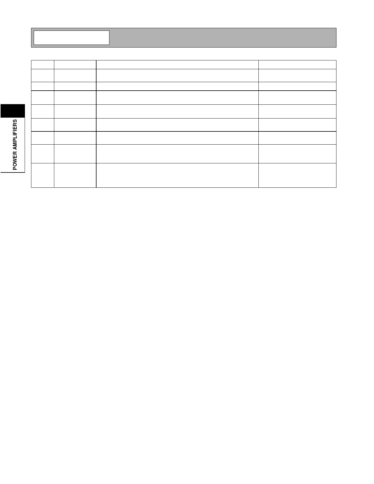
Pin Function Description
Interface Schematic
1
VCC1
First stage collector supply. A low frequency decoupling capacitor
(e.g., 4.7µF) is required.
2
RF IN
RF input internally matched to 50Ω. This input is internally AC-coupled.
3
VREG
Regulated voltage supply for amplifier bias. In Power Down mode, both
VREG and VMODE need to be LOW (<0.5V).
2
4
VMODE For nominal operation (High Power Mode), VMODE is set LOW. When
set HIGH, devices are turned off to improve efficiency.
5
VCC2
Output stage collector supply. A low frequency decoupling capacitor
(e.g., 4.7µF) is required.
6
RF OUT RF output internally matched to 50Ω. This output is internally
AC-coupled.
7
GND
Ground connection. Connect to package base ground. For best perfor-
mance, keep traces physically short and connect immediately to
ground plane.
Pkg
Base
GND
Ground connection. The backside of the package should be soldered to
a top side ground pad which is connected to the ground plane with mul-
tiple vias. The pad should have a short thermal path to the ground
plane.
2-272
Rev A3 011017
Share Link: 