CXB1558Q-Y Ver la hoja de datos (PDF) - Sony Semiconductor
Número de pieza
componentes Descripción
Lista de partido
CXB1558Q-Y Datasheet PDF : 11 Pages
| |||
Voltage Control Application
VSHUT
VCLK
TTL Level
Single Input
L: Shut down
Open High
ECL Level
Single Input
VEE = –5.2V
CXB1558Q-Y
0.01µF
24 23 22 21 20 19 18 17
VEE1 25
VEE = –5.2V
0.01µF VBB
26
ECL Level
Single Input
VIN
D 27
D 28
VCC1
29
IP
VDRIVADJ
P
30
200Ω P
31
32
DRIVADJ
510Ω
VOLTAGE
SOURCE
D-FF
INPUT SIGNAL
MONITOR
MODULATION
GENERATOR
1 23 4 5
BIAS
GENERATOR
678
16 NC
15 NC
14 NC
13 NC
12 NC
BIASADJ
11
510Ω
VEE2
10
SBIAS
9
VBIASADJ
VEE = –5.2V
A
IQMONITOR
A
IQ : IQMONITOR ≈ 11 : 1
VEE = –5.2V
5.1Ω
0.1µH
IQ
Laser
Diode
IBIAS
IBIASMONITOR
IBIAS : IBIASMONITOR ≈ 12 : 1
Cautions for Handling
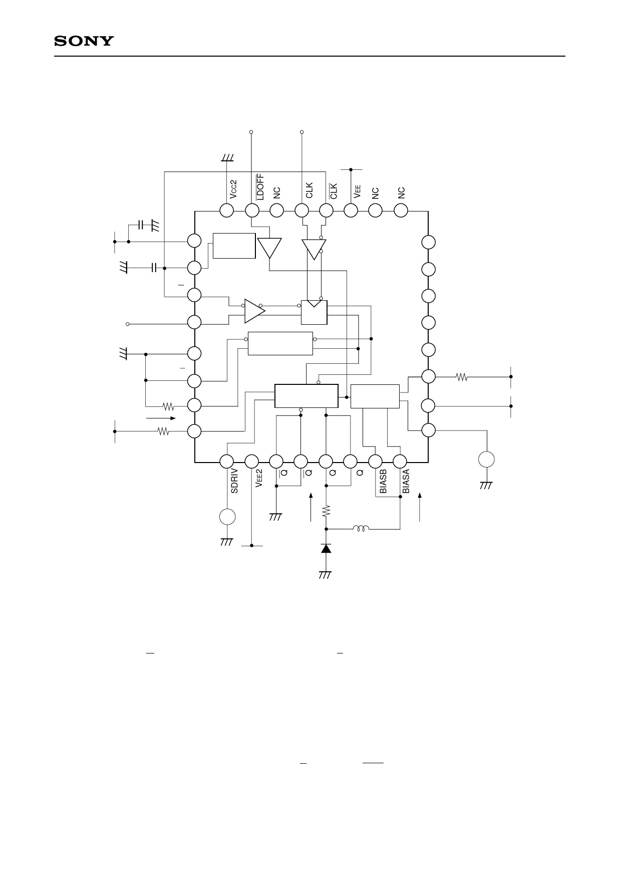
1. The outputs (Q, Q, BIASA, BIASB, SDRIV, SBIAS, P and P) on this IC are the open collector type.
Therefore, when these pins are not bing used, connect them to Vcc.
2. When the inputs (DRIVEADJ and BIASADJ) are not bing used, connect them to VEE.
3. Do not apply voltage over VEE + 2.5V to DRIVADJ pin and BIASADJ pin.
4. In voltage control Application, do not apply voltage over the output voltage range to SDRIV pin and SBIAS
pin. (see DC Characteristics of Laser Part and Voltage Control Application Circuit.)
5. Maximum drive current of VBB pin is ±200µA.
6. Maximum input differential voltage is 2.5V. ( | D – D | , | CLK – CLK | )
7. As the electronic breakdown level is weak, take care to handle.
–9–
Share Link: 