USB3300-EZK Ver la hoja de datos (PDF) - SMSC -> Microchip
Número de pieza
componentes Descripción
Lista de partido
USB3300-EZK Datasheet PDF : 55 Pages
| |||
Hi-Speed USB Host, Device or OTG PHY with ULPI Low Pin Interface
Datasheet
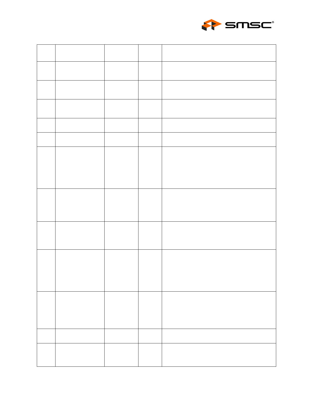
Table 3.1 USB3300 Pin Definitions 32-Pin QFN Package (continued)
DIRECTION, ACTIVE
PIN
NAME
TYPE
LEVEL DESCRIPTION
4
VBUS
I/O,
Analog
N/A VBUS pin of the USB cable. The USB3300 uses this
pin for the Vbus comparator inputs and for Vbus
pulsing during session request protocol.
5
ID
Input,
Analog
N/A ID pin of the USB cable. For non-OTG applications
this pin can be floated. For an A-Device ID = 0. For
a B-Device ID = 1.
6
VDD3.3
Power
N/A 3.3V Supply. A 0.1uF bypass capacitor should be
connected between this pin and the ground plane on
the PCB.
7
DP
I/O,
Analog
N/A D+ pin of the USB cable.
8
DM
I/O,
Analog
N/A D- pin of the USB cable.
9
RESET
Input, CMOS High Optional active high transceiver reset. This is the
same as a write to the ULPI Reset, address 04h, bit
5. This does not reset the ULPI register set. This pin
includes an integrated pull-down resistor to ground.
If not used, this pin can be floated or connected to
ground (recommended).
See Section 6.1.11, "Reset Pin" for details.
10
EXTVBUS
Input, CMOS High External Vbus Detect. Connect to fault output of an
external USB power switch or an external Vbus Valid
comparator. See Section 6.5.4, "External Vbus
Indicator," on page 44 for details. This pin has a pull
down resistor to prevent it from floating when the
ULPI bit UseExternalVbusIndicator is set to 0.
11
NXT
Output,
CMOS
High
The PHY asserts NXT to throttle the data. When the
Link is sending data to the PHY, NXT indicates when
the current byte has been accepted by the PHY. The
Link places the next byte on the data bus in the
following clock cycle.
12
DIR
Output,
CMOS
N/A Controls the direction of the data bus. When the
PHY has data to transfer to the Link, it drives DIR
high to take ownership of the bus. When the PHY
has no data to transfer it drives DIR low and
monitors the bus for commands from the Link. The
PHY will pull DIR high whenever the interface cannot
accept data from the Link, such as during PLL start-
up.
13
STP
Input,
CMOS
High
The Link asserts STP for one clock cycle to stop the
data stream currently on the bus. If the Link is
sending data to the PHY, STP indicates the last byte
of data was on the bus in the previous cycle. The
STP pin also includes the interface protection
detailed in Section 6.1.9.3, "Interface Protection," on
page 36.
14
CLKOUT
Output,
CMOS
N/A 60MHz reference clock output. All ULPI signals are
driven synchronous to the rising edge of this clock.
15
VDD1.8
Power
N/A 1.8V for digital circuitry on chip. Supplied by On-Chip
Regulator when REG_EN is active. Place a 0.1uF
capacitor near this pin and connect the capacitor
from this pin to ground. Connect pin 15 to pin 26.
SMSC USB3300
11
DATASHEET
Revision 1.08 (11-07-07)
Share Link: 