IN74HC651 Ver la hoja de datos (PDF) - Integral Corp.
Número de pieza
componentes Descripción
Lista de partido
IN74HC651
Integral Corp.

IN74HC651 Datasheet PDF : 9 Pages
| |||
TECHNICAL DATA
IN74HC651
Octal 3-State Bus Transceivers
and D Flip-Flops
High-Performance Silicon-Gate CMOS
The IN74HC651 is identical in pinout to the LS/ALS651. The
device inputs are compatible with standard CMOS outputs; with pullup
resistors, they are compatible with LS/ALSTTL outputs.
These devices consists of bus transceiver circuits, D-type flip-flop,
and control circuitry arranged for multiplex transmission of data
directly from the data bus or from the internal storage registers.
Direction and Output Enable are provided to select the read-time or
stored data function. Data on the A or B Data bus, or both, can be
stored in the internal D flip-flops by low-to-high transitions at the
appropriate clock pins (A-to-B Clock or B-to-A Clock) regardless of
the select or enable or enable control pins. When A-to-B Source and
B-to-A Source are in the real-time transfer mode, it is also possible to
ORDERING INFORMATION
IN74HC651N Plastic
IN74HC651DW SOIC
TA = -55° to 125° C for all packages
store data without using the internal D-type flip-flops by simulta-
neously enabling Direction and Output Enable. In this configuration
each output reinforces its input. Thus, when all other data sources to the two sets of bus lines are at high
impedance, each set of bus lines will remain at its last state.
The IN74HC651 has inverted outputs.
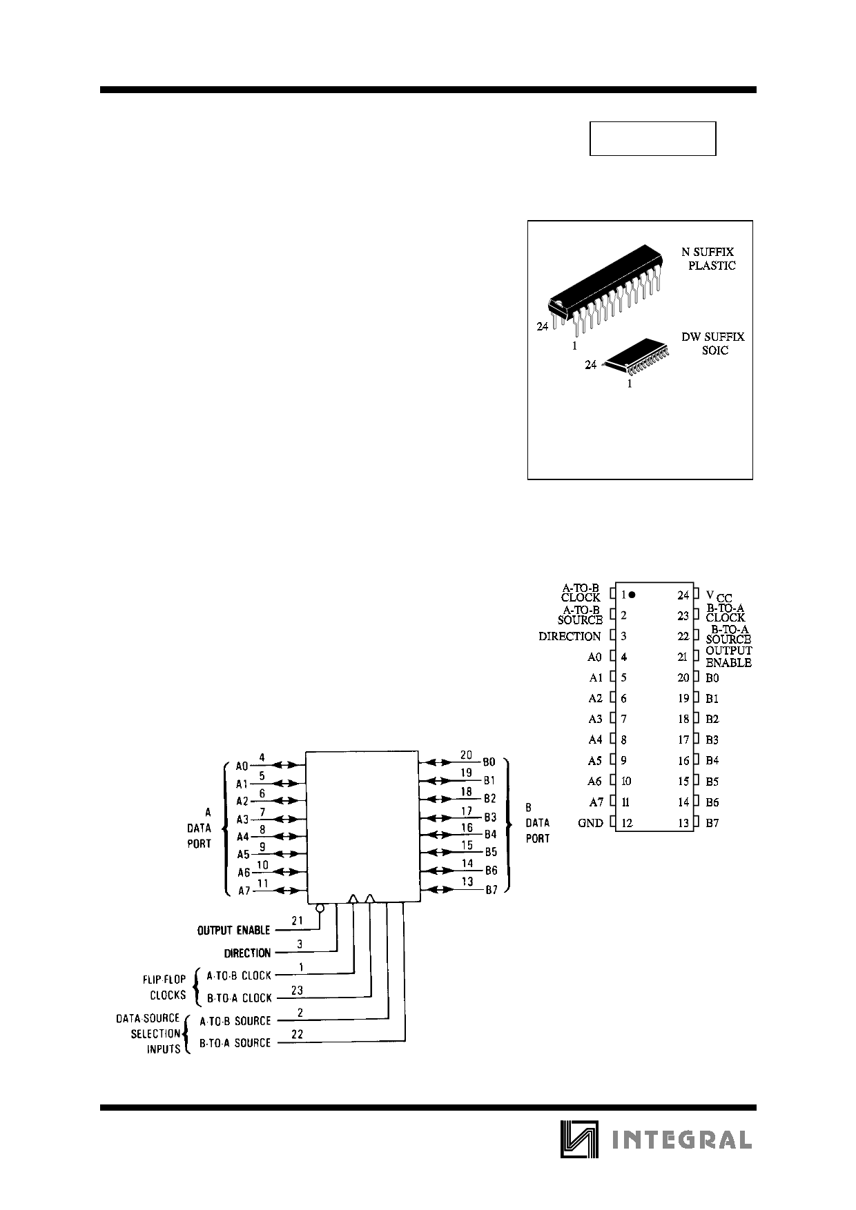
PIN ASSIGNMENT
• Outputs Directly Interface to CMOS, NMOS, and TTL
• Operating Voltage Range: 2.0 to 6.0 V
• Low Input Current: 1.0 µA
• High Noise Immunity Characteristic of CMOS Devices
LOGIC DIAGRAM
PIN 24=VCC
PIN 12 = GND
456
Share Link: