LA8633V Ver la hoja de datos (PDF) - SANYO -> Panasonic
Número de pieza
componentes Descripción
Lista de partido
LA8633V Datasheet PDF : 7 Pages
| |||
LA8633V
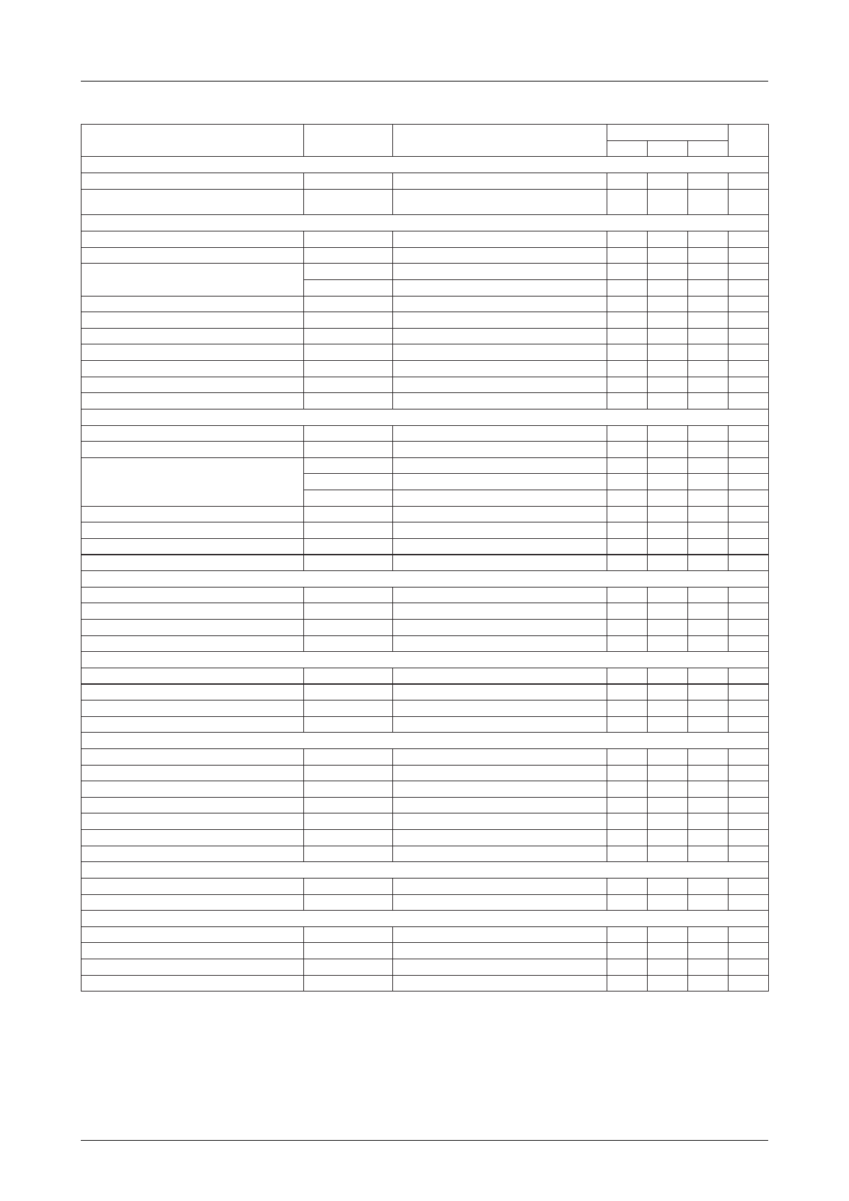
Electrical Characteristics
Parameter
Symbol
Conditions
Ratings
Unit
min
typ
max
[Supply current] Ta=25°C, VCC=3V, VB1=1.2V, f=1kHz
Current drain with no signal
ICCO
Standby current
ISTBY
No signal
No signal, data shaper ON (pin 9=H), standby
mode (pin 12=L)
2.5
3.4
5.0 mA
300 500 700 µA
[Compressor] Vinrefe=10mVrms=0dB, Pre AMP Gain=20dB, Output : pin 18, RL=10kΩ
Input impedance
rI
COUT rms output voltage
VOC
VI=Vinrefe=0dB
Gain error
Gec1
Gec2
VI=–20dB
VI=–40dB
Total harmonic distortion
THD
VI=0dB
COUT rms output noise voltage
VNOC
Rg=620Ω, f=20Hz to 20kHz
Limiting voltage
VL
Maximum preamplifier voltage gain
VGP max
Data voltage gain
VGD
Mute attenuation
ATTC
VI=0dB
Crosstalk
CTC
Expander rms input voltage=100mV
[Expander] Vinrefe=10mVrms=0dB, Filter AMP Gain=0dB, RL=10kΩ
Expander rms output voltage
VOE
VI=Vinrefe=0dB
Maximum expander rms output voltage
VO max
THD=10%, RL=10kΩ
Gee1
VI=5dB
Gain error
Gee2
VI=–20dB
Gee3
VI=–30dB
Total harmonic distortion
THD
VI=0dB, data shaper ON (pin 9=H)
Expander rms output noise voltage
VNOe
Rg=620Ω, f=20Hz to 20kHz
Mute attenuation
ATTe
VI=0dB
Crosstalk
CTe
50
kΩ
210 265 335 mVrms
–0.5
0.0 +0.5 dB
–1.0
0.0 +1.0 dB
0.25 1.00 %
1.5
3.0 mVrms
1.25 1.40 1.55 Vp-p
28
dB
–2
0
+2 dB
–60 –73
dB
–25 –34
dB
100 125
600 1000
–0.5
0
–1.0
0
–1.5
0
0.40
13
–60 –70
–60 –83
160 mVrms
mVrms
+0.5 dB
+1.0 dB
+2.0 dB
1.00 %
80 µVrms
dB
dB
[Compressor lowpass filter]
Input/output ratio
f=3.4kHz
–3
dB
Attenuation
Total harminic distortion
ATT
THD
Vin=10mVrms (in : 15pin)
–18
0.15
dB/octave
1.00 %
Maximum LPF2OUT rms output voltage
[Expander lowpass filter]
VO max
THD=10%, RL=10kΩ
600 1000
mVrms
Input/output ratio
f=3.4kHz
–3
dB
Attenuation
Total harminic distortion
ATT
THD
Vin=10mVrms
–18
0.35
dB/octave
1.00 %
Maximum LPF1OUT rms output voltage
[Frequency-shifted keyd comparator]
VO max
THD=10%, RL=7.7kΩ
200 340
mVrms
CCGCTL duty cycle
CHGCTL ON voltage
CHGCTL OFF voltage
CHGCTL input impedance
VHOLD input/output current
FSKOUT LOW-level output voltage
FSKOUT HIGH-level output voltage
[Standby mode characteristics]
Duty
VON
VOFF
RI
IIO
VOL
VOH
VIN=100mVrms
Pin 9
Pin 9
Pin 9
Pin7, pin9=2V
RL=100kΩ, pin10
RL=100kΩ, pin10
43
48
1
200
80
2.8
53 %
V
0.4 V
kΩ
µA
0.3 V
V
STBY voltage
STBY output current
[Digital input characteristics]
VSTBY
ISTBY
Pin 12
Pin 12, flowing out current
0.7 V
50 µA
Input L-level voltage
Input H-level voltage
Input L-level current
Input H-level current
VIL
Pins16, 17
VIH
Pins16, 17
IIL
VI=0.2V, Pins16, 17
IIH
VI=2V, Pins16, 17
0.6VCC
0.65 V
V
100 µA
5 µA
Note 1 : This IC enters mute mode when the pins 16 and 17 become low.
2 : Pin 6 is used as an output pin when 8 is high (=open), pin 5 is used as an output pin when pin 8 is low.
3 : FSK waveform shaper circuit becomes on when pin 9 is high.
4 : FSK waveform shaping polarity : outputs low in the positive cycle of signal.
No.4078–2/7
Share Link: 