MD1320N Ver la hoja de datos (PDF) - Unspecified
Número de pieza
componentes Descripción
Lista de partido
MD1320N Datasheet PDF : 2 Pages
| |||
3.3V/5V Output MD1320N
32
Company Name
14.1MAX
13.6 +– 0.1
Dimensions = mm
17
Type No.
SHINDENGEN
MD1320N
5038N
1
(0.8)
16
Lot No.
0.35 +– 0.1 0.16 M
0.8
DESCRIPTION
The MD1320N is a high-efficiency step down DC-DC converter
power integrated circuit with main MOSFET switch and Schottky
Barrier Diode. The MD1320N can deliver 7.5 watts maximum
(5V, 1.5A) with high efficiency over a wide input voltage range.
This device has output voltage digitally selectable for 3.3V or 5V.
With the MD1320N you can construct a complete DC-DC converter
using only a few external components. Featuring an SSOP 32-pin
surface mount package, the MD1320N allows you to incorporate
a very small and thin power supply on your circuit board.
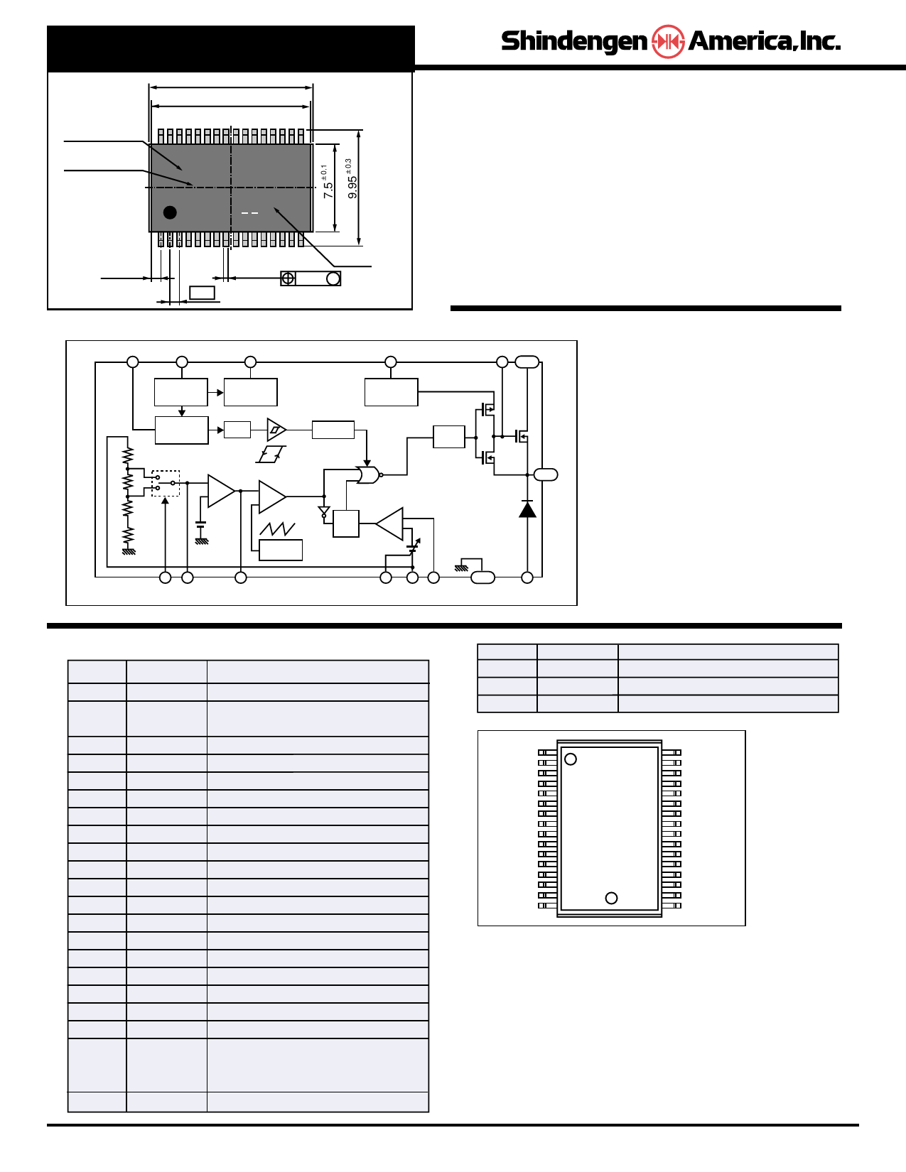
BLOCK DIAGRAM
Vref
28
Vcc
6
UVLO
START =7.5V
STOP =7V
Vboot
8
BOOT Reference
Vref=6.5V
VB
25
Driver
Vref=Vout+10V
VG VDD
23 18~21
Reference
Vref=5V+–5%
TSD
Main Switch
MOS OFF
3.3V F/B
5.0V F/B
Error amp
–
+
100˚C
150˚C
PWM Comp
+
–
2.5V
3V
1V
OSC
f=250kHz
Q
+
RS
–
CLM Vth=
0.1~0.2V
Driver
27 28
3.3V/5V amp–
27
ampOUT
1
2
3
S/S F/B OCL– OCL+
4,26
GND
VOUT
11~14
16
P.GND
FEATURES
" High efficiency typ. 91%
" Wide input voltage load range
8VDC to 30VDC
Up to 1.5ADC
" Output voltage selectable function
3.3V or 5V digitally
" Internal Switching power device
Main MOSFET for switch
SBD for rectification
" Fixed 250kHz PWM frequency
Without external resistor and capacitor
" Overcurrent protection
" Thermal shutdown function
PIN ASSIGNMENT
Pin#
1
2
3
4
5
6
7
8
9,10
11 ~ 14
15
16
17
18 ~ 21
22
23
24
25
26
27
28
Symbol
S/S
F/B OCL-
OCL+
GND
N/C
Vcc
N/C
Vboot
N/C
VOUT
N/C
P.GND
N/C
VDD
N/C
VG
N/C
VB
GND
3.3V/5V
Vref
AmpOUT
Vref
Function description
Capacitor for softstart
Overcurrent protection (OCL) (-)
and output voltage feedback
Overcurrent protection (OCL) (+)
Signal GND
Non-connection
Input voltage
Non-connection
High side drive supply for main MOS
Non-connection
Power stage output
Non-connection
Power GND
Non-connection
Drain of main MOS Switch
Non-connection
Gate terminal of main MOS
Non-connection
Bootstrap capacitor between VB and VOUT
Signal GND
Output voltage selectable terminal
“L” means 5V output voltage
“H” means 3.3V output voltage
Internal voltage reference
29
N/C
Non-connection
30
AmpOUT
Error Amp out
31
N/C
Non-connection
32
amp-
Error Amp (-) input
S/S : 1
F/B OCL– : 2
OCL+ : 3
GND : 4
N/C : 5
VCC : 6
N/C : 7
Vboot : 8
N/C : 9
N/C : 10
VOUT: 11
VOUT: 12
VOUT: 13
VOUT: 14
N/C : 15
P.GND : 16
32 : amp-
31 : N/C
30 : ampOUT
29 : N/C
28 : Vref
27 : 3.3V/5V
26 : GND
25 : VB
24 : N/C
23 : VG
22: N/C
21: VDD
20: VDD
19: VDD
18 : VDD
17 : N/C
" Vref - Temperature compensated internal voltage. You can pull 1mA
maximum for external circuit.
" OSC - MCD1320N uses internal oscillator without external component.
Frequency (Saw tooth wave form) is trimmed to 250kHz on chip.
" Error Amp - Error Amp detects output voltage of DC-DC converter
and controls PWM signal. You can adjust the loop gain when you
connect feedback resistor and capacitor between AmpOUT and
Amp (-). It will provide stable phase compensation.
" Overcurrent protection - MD1320N uses pulse-by-pulse current
protection. Current will be sensed voltage drop of external current
sensing resistor. Threshold of OCL is 0.19V.
1-800-634-3654
Share Link: 