IRF620 Ver la hoja de datos (PDF) - New Jersey Semiconductor
Número de pieza
componentes Descripción
Lista de partido
IRF620 Datasheet PDF : 2 Pages
| |||
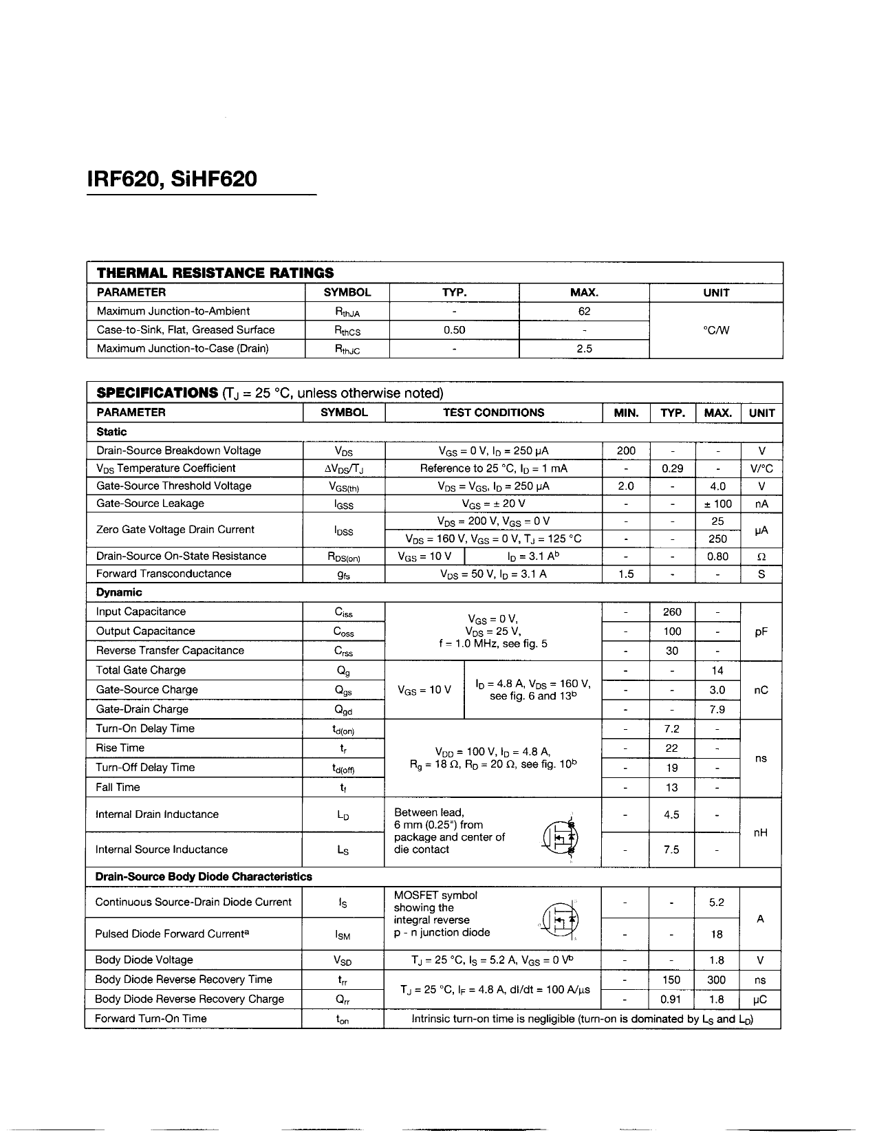
IRF620, SIHF620
THERMAL RESISTANCE RATINGS
PARAMETER
SYMBOL
Maximum Junction-to-Ambient
RthJA
Case-to-Sink, Flat, Greased Surface
RthCS
Maximum Junction-to-Case (Drain)
RthJC
TYP.
-
0.50
-
MAX.
62
-
2.5
UNIT
°c/w
SPECIFICATIONS (Tj = 25 °C, unless otherwise noted)
PARAMETER
SYMBOL
TEST CONDITIONS
MIN. TYP.
MAX.
UNIT
Static
Drain-Source Breakdown Voltage
VDS Temperature Coefficient
Gate-Source Threshold Voltage
Gate-Source Leakage
Zero Gate Voltage Drain Current
Drain-Source On-State Resistance
Forward Transconductance
Dynamic
VDS
AVDS/Tj
VQS(th)
bss
IDSS
RcS(on)
9fs
VGS = 0 V, ID = 250 uA
Reference to 25 °C, ID = 1 mA
VDS = VGS, ID = 250 uA
VGS = ± 20 V
VDS = 200 V, VGS = 0 V
VDS = 160 V, VGS = 0 V, Tj = 125 °C
VGS = 10V
!D = 3.1Ab
VDS = 50V,b = 3.1 A
200
-
-
0.29
-
V
- v/°c
2.0
-
4.0
V
-
-
±100
nA
-
-
25
uA
-
-
250
-
-
0.80
n
1.5
-
-
5
Input Capacitance
Output Capacitance
Reverse Transfer Capacitance
Total Gate Charge
Gate-Source Charge
Gate-Drain Charge
Turn-On Delay Time
Q55
Coss
Cres
Qg
Qgs
Q9d
td(on)
VGS - 0 V,
-
VDS = 25 V,
-
f = 1 .0 MHz, see fig. 5
-
-
Vrs-10V
VGS-TUV
b -4.8 A,VDS -160V,
see fig. 6 and 13b
-
-
-
260
-
100
-
PF
30
-
-
14
-
3.0
nC
-
7.9
7.2
-
Rise Time
Turn-Off Delay Time
tr
'd(off)
VDD=100V, ID = 4.8 A,
Rg = 18 n, RD = 20O, seefig. 10b
-
22
-
ns
-
19
-
Fall Time
tf
-
13
-
Internal Drain Inductance
Internal Source Inductance
LD
Between lead,
-
4.5
-
6 mm (0.25") from
s\
4
package and center of
(I NI Tj
nH
Ls
die contact
vll^*
-
7.5
-
Drain-Source Body Diode Characteristics
Continuous Source-Drain Diode Current
Is
Pulsed Diode Forward Current3
ISM
MOSFET symbol
showing the
integral reverse
p - njunction diode
/fjZik
(,(J j*]_t)
xtif
-
-
5.2
A
-
-
18
Body Diode Voltage
VSD
Body Diode Reverse Recovery Time
trr
Body Diode Reverse Recovery Charge
Qrr
Forward Turn-On Time
ton
Tj = 25 °C, ls = 5.2 A, VGS = 0 V»
-
-
1.8
V
-
150
300
ns
-
0.91
1.8
uC
Intrinsic turn-on time is negligible (turn-on is dominated by LS and LD)
Share Link: 