UT54ACS164245SEI Ver la hoja de datos (PDF) - Aeroflex Corporation
Número de pieza
componentes Descripción
Lista de partido
UT54ACS164245SEI Datasheet PDF : 16 Pages
| |||
IO GUIDELINES
All inputs are 5 volt tolerant. When VDD2 is at 3.3 volts, either
3.3 or 5 volt CMOS logic levels can be applied to all control in-
puts. It is recommended that all unused inputs be tied to VSS
through a 1KΩ to 10KΩ resistor.
It's good design practice to tie the unused input to VSS via a re-
sistor to reduce noise susceptibility. The resistor protects the in-
put pin by limiting the current from high going variations in
VSS.
The number of inputs that can be tied to the resistor pull-down
can vary. It is up to the system designer to choose how many
inputs are tied together by figuring out the max load the part can
drivewhile still meeting system performance specs. Input signal
transitions should be driven to the device with a rise
and fall time that is <100ms.
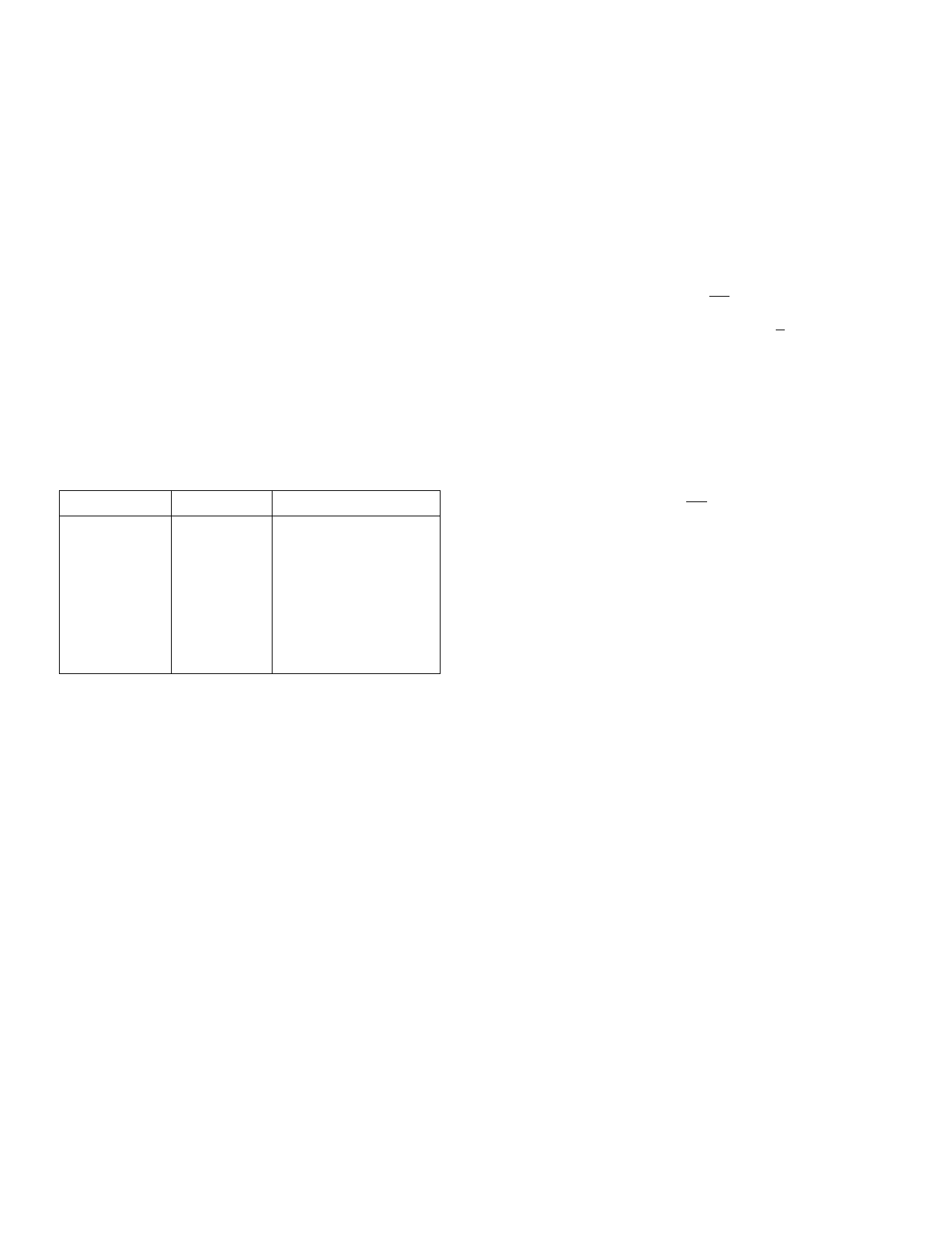
POWER TABLE
Port B
Port A
5 Volts
3.3 Volts
5 Volts
5 Volts
3.3 Volts
3.3 Volts
VSS
VSS
3.3V or 5V
VSS
3.3V or 5V
VSS
OPERATION
Voltage Translator
Non Translating
Non Translating
Cold Spare
Port A Warm Spare
Port B Warm Spare
POWER APPLICATION GUIDELINES
For proper operation, connect power to all VDD pins and ground
all VSS pins (i.e., no floating VDD or VSS input pins). By virtue
of the UT54ACS164245SEI warm spare feature, power supplies
VDD1 and VDD2 may be applied to the device in any order. To
ensure the device is in cold spare mode, both supplies, VDD1 and
VDD2 must be equal to VSS +/- 0.3V. Warm spare operation is
in effect when one power supply is >1V and the other power
supply is equal to VSS +/- 0.3V. If VDD1 has a power on ramp
longer than 1 second, then VDD2 should be powered on first to
ensure proper control of DIRx and OEx. During normal opera-
tion of the part, after power-up, ensure VDD1>VDD2.
By definition, warm sparing occurs when half of the chip re-
ceives its normal VDD supply value while the VDD supplying the
other half of the chip is set to 0.0V. When the chip is "warm
spared", the side that has VDD set to a normal operational value
is "actively" tri-stated because the chip’s internal OE signal is
forced low. The side of the chip that has VDD set to 0.0V is "pas-
sively" tri-stated by the cold spare circuitry. In order to mini-
mize transients and current consumption, the user is encouraged
to first apply a high level to the OEx pins and then power down
the appropriate supply.
3
Share Link: 