SPX2975R5-5.0 Ver la hoja de datos (PDF) - Signal Processing Technologies
Número de pieza
componentes Descripción
Lista de partido
SPX2975R5-5.0 Datasheet PDF : 11 Pages
| |||
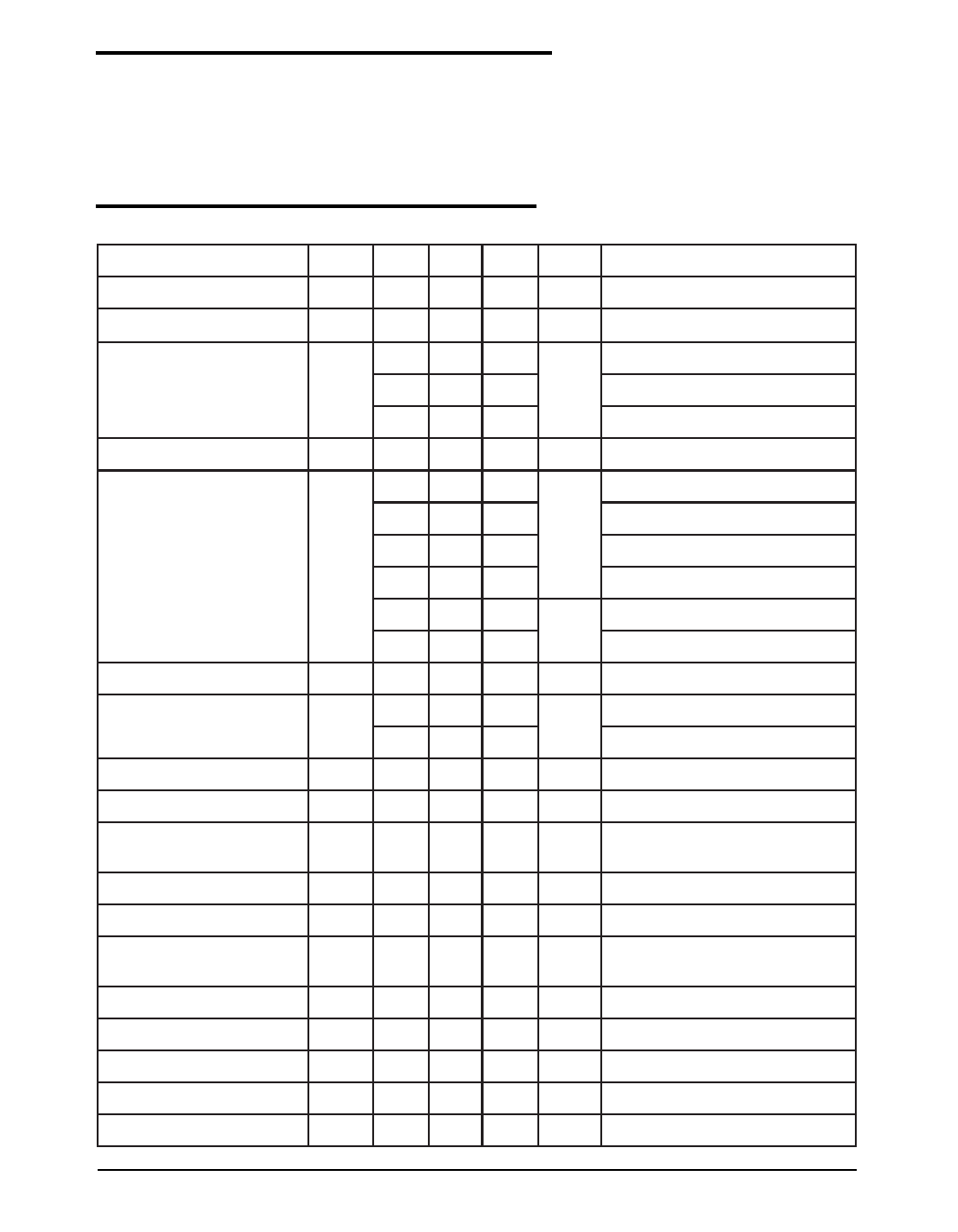
Input Voltage ...................................................................... -42V to 45V
Output Voltage .................................................................... -1.0 to 16V
Output Current ............................................................ Internally limited
Reset Output Voltage .......................................................... -0.3 to 25V
Reset Output Current ..................................................... -5mA to +5mA
Reset Delay Voltage ........................................................ -0.3V to 7.0V
Reset Delay Current ......................................................... -2mA to 2mA
Storage Temperature .................................................. -50°C to +150°C
Junction Temperature.(Note 1) ................................... -40°C to +150°C
ABSOLUTE MAXIMUM RATINGS
TJA (TO-252)............................................................................... 78°C/W
TJA (TO-220)............................................................................... 65°C/W
TJA (TO-263)............................................................................... 53°C/W
TJC (TO-220, T0 263, and TO-252).............................................. 4°C/W
These are stress ratings only and functional operation of the device at
these ratings or any other above those indicated in the operation sections
of the specifications below is not implied. Exposure to absolute maximum
rating conditions for extended periods of time may affect reliability.
VIN = 13.5V; -40°C < Tj < 150°C. Unless otherwise specified.
ELECTRICAL CHARACTERISTICS
PARAMETER
SYM MIN. TYP. MAX. UNITS
CONDITIONS
Input Voltage
VI
5.5
42
V
Junction Temperature
TJ
-40
150
ºC
4.9 5.0 5.1
5mA < IQ < 400mA, 6V < VI < 28V
Output Voltage
VQ
4.9 5.0 5.1
V 5mA < IQ < 200mA, 6V < VI < 40V
4.9
5.25
100µA ≤ IQ ≤ 5mA, 6V < VI < 28V
Output Current limitation
IQ
450 700
mA
60 100
IOUT = 100 µA, Tj = 25ºC
Current Consumption
Iq
60 120
IOUT = 100 µA, Tj = 85ºC
µA
70 180
IOUT = 1mA, Tj = 25ºC
70 200
IOUT = 1mA, Tj = 85ºC
7
10
IOUT = 250mA
mA
17 22
IOUT = 400mA
Dropout Voltage (note 1)
Vdr
350 500
mV IOUT = 300mA, VDO = VOUT - VIN
Load Regulation
-30
∆VQ
5
30
IOUT = 5mA to 400mA
mV
-200
200
IOUT =100µA ≤ IQ ≤ 5mA
Line Regulation
∆VQ
-15
2
15
mV VIN = 8V to 32V, IOUT = 5mA
PSRR
PSRR
60
dB fr = 100Hz; Vr = 0.5 Vpp
Temperature Output Voltage
Drift
dVQ/dT
0.2
mV/K
Reset Switching Threshold
Reset Output Low Voltage
Reset Output Leakage
Current
VRT
VRQL
IRQH
4.51 4.65 4.8
0.2 0.4
0
10
V
VTH
V
Rext ≥ 5kΩ ; VOUT > 1 V
µA
VROH = 5V
Reset Charging Current
ID
3.0 5.5 9.0
µA VRD = 1V
Upper Timing Threshold
VDU
1.5 1.8 2.2
V
VthH
Lower Timing Threshold
VDL
0.2 0.4 0.7
V
VthL
Reset Delay Time
td
10 16 22
ms CO = 47nF, Td
Reset Reaction Time
tRR
0.5 2.0
µs CO = 47nF, Trv
Note 1: Measured when the output voltage (Vout) has dropped 100mV form the nominal value obtained at Vin=13.5V
Date: 1/17/05
SPX2975 400mA Low Dropout Voltage Regulator
2
© Copyright 2005 Sipex Corporation
Share Link: 