LM79L05M3 Ver la hoja de datos (PDF) - Cystech Electonics Corp.
Número de pieza
componentes Descripción
Lista de partido
LM79L05M3 Datasheet PDF : 8 Pages
| |||
CYStech Electronics Corp.
Spec. No. : C508M3
Issued Date : 2006.07.12
Revised Date : 2013.08.12
Page No. : 4/8
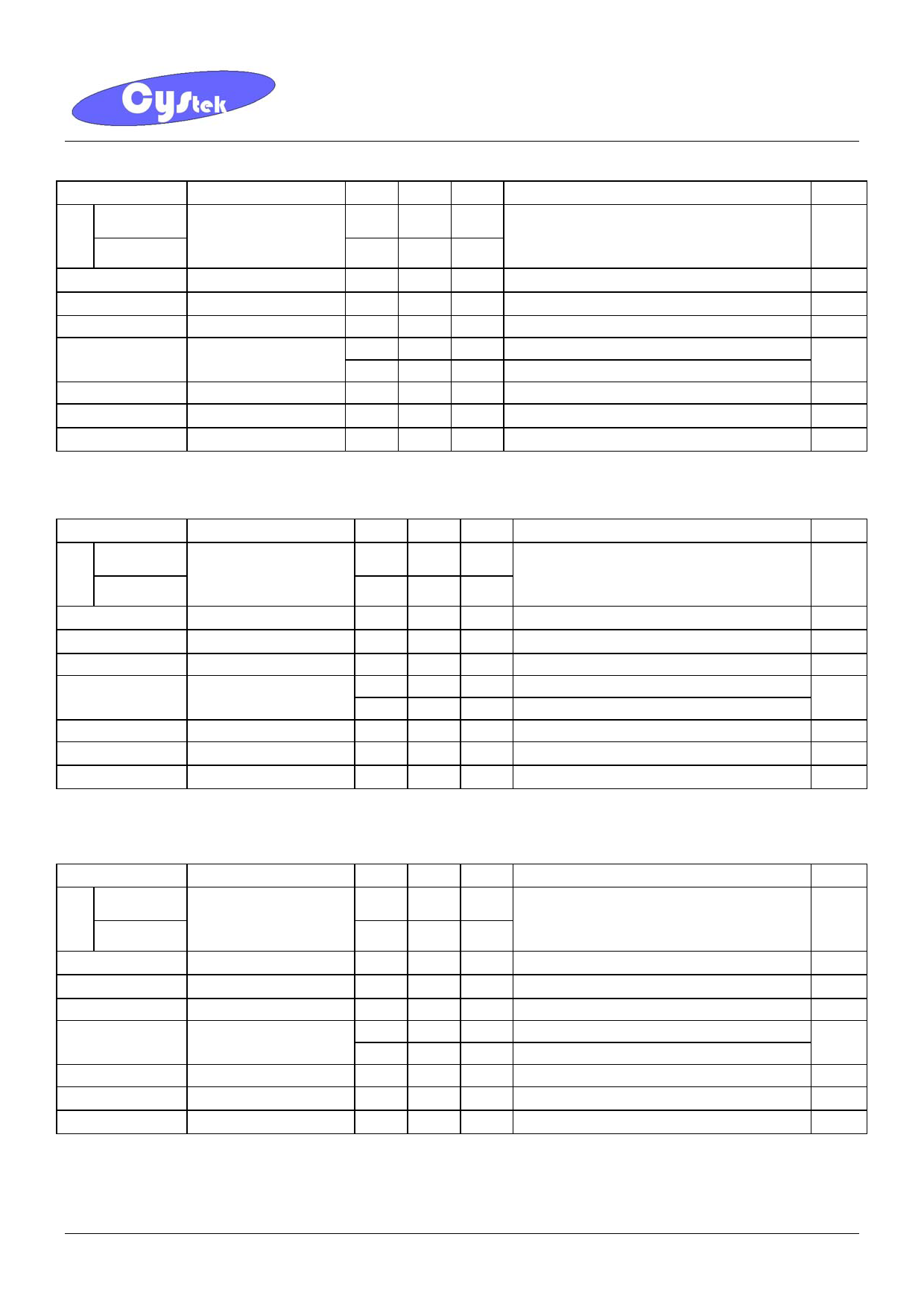
LM79L15 (Vin=-23V, Io=40mA, Tj=0~125°C, Cin=0.33μF, Cout=0.1μF, unless otherwise noted) (Note 1)
Symbol
Parameter
Min Typ Max
Conditions
Units
A-rank(3%)
-14.55 -15 -15.45 Vin=-23V, Io=40mA,Tj=25°C
Vo
Output Voltage
-17.5V≤Vin≤-30V, 1mA≤Io≤40mA
V
B-rank(5%)
-14.25 - -15.75 Vin=-23V,1mA≤Io≤70mA (Note 2)
ΔVo
Line Regulation
- 65 300 -17.5V≤Vin≤-30V, Tj=25°C
mV
ΔVo
Load Regulation
- 25 150 1mA≤Io≤100mA, Tj=25°C
mV
IQ
Quiescent Current
-
- 6.5 Vin=-23V, Io=40mA, Tj=25°C
mA
ΔIQ
Quiescent Current
Change
-
- 1.5 -20V≤Vin≤-30V
-
- 0.1 1mA≤Io≤40mA
mA
Vn
Output Noise Voltage - 90 - 10Hz≤f≤100KHz
μV
ΔVin / ΔVout Ripple Rejection
34 39 - -18.5V≤Vin≤-28.5V, f=120Hz, Tj=25°C
dB
VD
Dropout Voltage
- 1.7 - Io=100mA, Tj=25°C
V
LM79L18 (Vin=-27V, Io=40mA, Tj=0~125°C, Cin=0.33μF, Cout=0.1μF, unless otherwise noted) (Note 1)
Symbol
Parameter
Min Typ Max
Conditions
Units
A-rank(3%)
-17.46 -18 -18.54 Vin=-27V, Io=40mA,Tj=25°C
Vo
Output Voltage
-20.5V≤Vin≤-33V, 1mA≤Io≤40mA
V
B-rank(5%)
-17.10 - -18.90 Vin=-27V,1mA≤Io≤70mA (Note 2)
ΔVo
Line Regulation
- 70 300 -20.5V≤Vin≤-33V, Tj=25°C
mV
ΔVo
Load Regulation
- 27 170 1mA≤Io≤100mA, Tj=25°C
mV
IQ
Quiescent Current
-
- 6.5 Vin=-27V, Io=40mA, Tj=25°C
mA
ΔIQ
Quiescent Current
Change
-
- 1.5 -21V≤Vin≤-33V
-
- 0.1 1mA≤Io≤40mA
mA
Vn
Output Noise Voltage - 150 - 10Hz≤f≤100KHz
μV
ΔVin / ΔVout Ripple Rejection
33 48 - -23V≤Vin≤-33V, f=120Hz, Tj=25°C
dB
VD
Dropout Voltage
- 1.7 - Io=100mA, Tj=25°C
V
LM79L24 (Vin=-33V, Io=40mA, Tj=0~125°C, Cin=0.33μF, Cout=0.1μF, unless otherwise noted) (Note 1)
Symbol
Parameter
Min Typ Max
Conditions
Units
A-rank(3%)
-23.28 -24 -24.72 Vin=-33V, Io=40mA,Tj=25°C
Vo
Output Voltage
-27V≤Vin≤-38V, 1mA≤Io≤40mA
V
B-rank(5%)
-22.80
-25.20 Vin=-33V,1mA≤Io≤70mA (Note 2)
ΔVo
Line Regulation
- 90 350 -27V≤Vin≤-38V, Tj=25°C
mV
ΔVo
Load Regulation
- 40 200 1mA≤Io≤100mA, Tj=25°C
mV
IQ
Quiescent Current
-
- 6.5 Vin=-33V, Io=40mA ,Tj=25°C
mA
ΔIQ
Quiescent Current
Change
-
- 1.5 -28V≤Vin≤-38V
-
- 0.1 1mA≤Io≤40mA
mA
Vn
Output Noise Voltage - 200 - 10Hz≤f≤100KHz
μV
ΔVin / ΔVout Ripple Rejection
31 47 - -29V≤Vin≤-35V, f=120Hz, Tj=25°C
dB
VD
Dropout Voltage
- 1.7 - Io=100mA, Tj=25°C
V
Note : 1. The maximum steady state usable output current is dependent on input voltage, heat sinking, lead length of the package
and copper of PCB. The data above represent pulse test conditions with junction temperatures specified at the initial of
test.
2. Power dissipation<0.5W
LM79LXXM3
CYStek Product Specification
Share Link: 