ML9059E Ver la hoja de datos (PDF) - LAPIS Semiconductor Co., Ltd.
Número de pieza
componentes Descripción
Lista de partido
ML9059E
LAPIS Semiconductor Co., Ltd.

ML9059E Datasheet PDF : 72 Pages
| |||
LAPIS Semiconductor
FEDL9059E-01
ML9059E
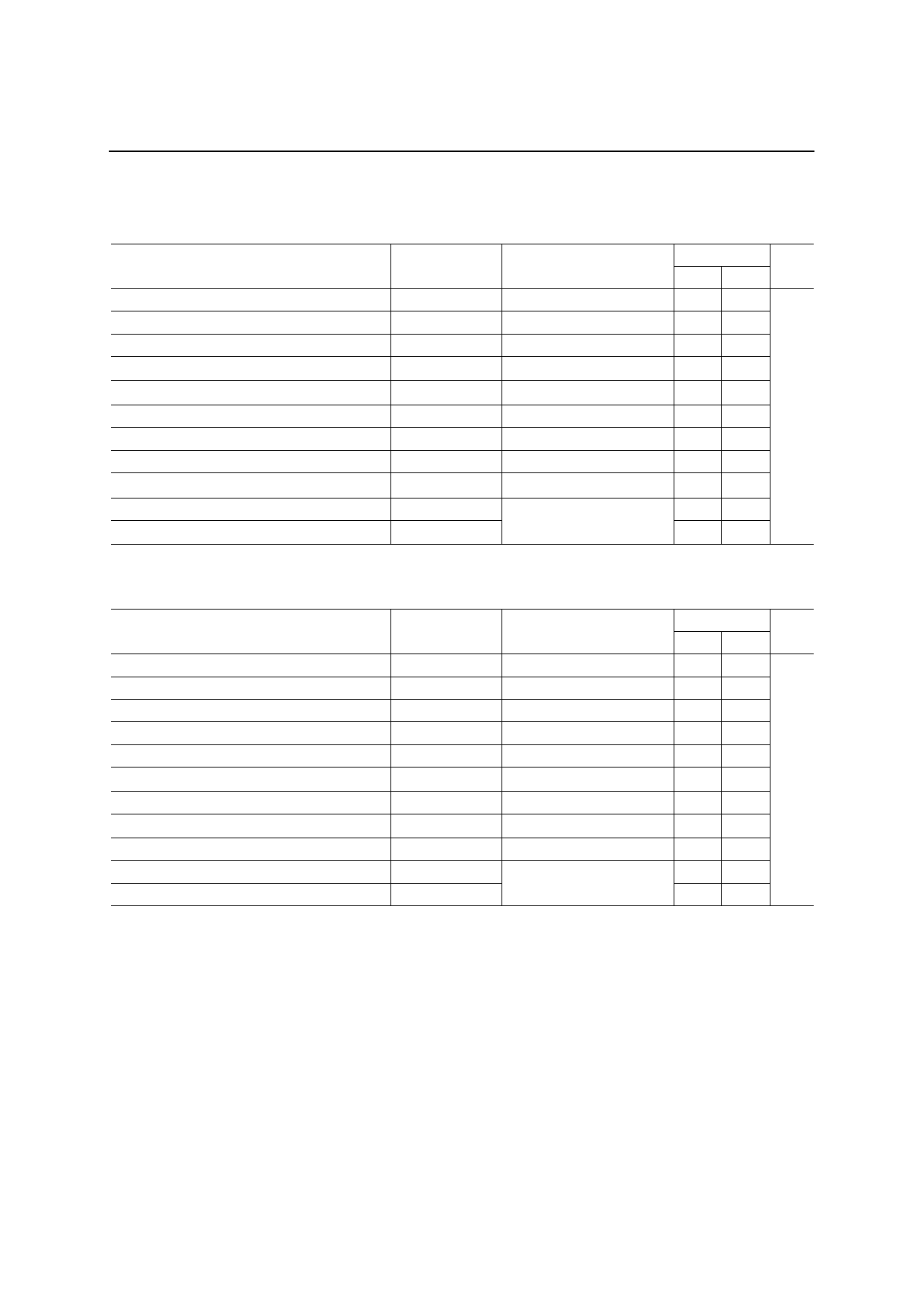
Parameter
Address hold time
Address setup time
System cycle time
Control L pulse width (WR)
Control L pulse width (RD)
Control H pulse width (WR)
Control H pulse width (RD)
Data setup time
Data hold time
RD Access time
Output disable time
Symbol
tAH8
tAW8
tCYC8
tCCLW
tCCLR
tCCHW
tCCHR
tDS8
tDH8
tACC8
tOH8
[VDD = 4.5 to 5.5 V, Tj = –40 to +85°C]
Condition
Rated value
Unit
Min Max
5
—
5
—
166 —
30 —
70 —
55 — ns
55 —
30 —
10 —
CL = 100 pF
— 70
5
50
Parameter
Address hold time
Address setup time
System cycle time
Control L pulse width (WR)
Control L pulse width (RD)
Control H pulse width (WR)
Control H pulse width (RD)
Data setup time
Data hold time
RD Access time
Output disable time
Symbol
tAH8
tAW8
tCYC8
tCCLW
tCCLR
tCCHW
tCCHR
tDS8
tDH8
tACC8
tOH8
[VDD = 3.7 to 4.5 V, Tj = –40 to +85°C]
Condition
Rated value
Unit
Min Max
5
—
5
—
300 —
60 —
120 —
60 — ns
60 —
40 —
15 —
CL = 100 pF
— 140
10 100
Note 1:
Note 2:
Note 3:
The input signal rise and fall times are specified as 15ns or less.
When using the system cycle time for fast speed, the specified values are (tr + tf) (tCYC8 –
tCCLW – tCCHW) or (tr + tf) (tCYC8 – tCCLR – tCCHR).
All timings are specified taking the levels of 20% and 80% of VDD as the reference.
The values of tCCLW and tCCLR are specified during the overlapping period of CS1 at “L” (CS2 =
“H”) and the “L” levels of WR and RD, respectively.
9/72
Share Link: