ML9208-XXGA Ver la hoja de datos (PDF) - LAPIS Semiconductor Co., Ltd.
Número de pieza
componentes Descripción
Lista de partido
ML9208-XXGA
LAPIS Semiconductor Co., Ltd.

ML9208-XXGA Datasheet PDF : 33 Pages
| |||
FEDL9208-02
ML9208
PIN DESCRIPTION
Pin
Symbol Type Connects to
QFP SSOP
Description
1 to 31,
5 to 39 SEG1 to 35 O
61 to 64
Fluorescent
tube anode
electrode
Fluorescent display tube anode electrode drive output.
Directly connected to fluorescent display tube and a
pull-down resistor is not necessary. IOH > –6 mA
32 to 47 40 to 55 COM1 to 16 O
59, 60 3, 4 AD1, AD2 O
Fluorescent
tube grid
electrode
Fluorescent
tube anode
electrode
Fluorescent display tube grid electrode drive output.
Directly connected to fluorescent display tube and a
pull-down resistor is not necessary. IOH > –30 mA
Fluorescent display tube anode electrode drive output.
Directly connected to fluorescent display tube and a
pull-down resistor is not necessary. IOH > –15 mA
57, 58 1, 2
P1, P2
General port output.
LED drive
O control pins Output of these pins in static operation, so these pins can
drive the LED.
56
64
49
57
48
56
VDD
GND
VFL
VDD-GND are power supplies for internal logic.
— Power supply VDD-VFL are power supplies for driving fluorescent tubes.
Apply VFL after VDD is applied.
Serial data input (positive logic).
55
63
DA
I Microcontroller
Input from LSB.
54
62
CP
Shift clock input.
I Microcontroller Serial data is shifted on the rising edge of CP.
53
61
CS
Chip select input.
I Microcontroller Serial data transfer is disabled when CS pin is “H” level.
Reset input.
“Low” initializes all the functions.
Initial status is as follows.
Address of each RAM address “00”H
Data of each RAM Content is undefined
Display digit 16 digits
52
60
RESET
I Microcontroller Contrast adjustment 8/16
or C2, R2
All lights ON or OFF OFF mode
All outputs “Low” level
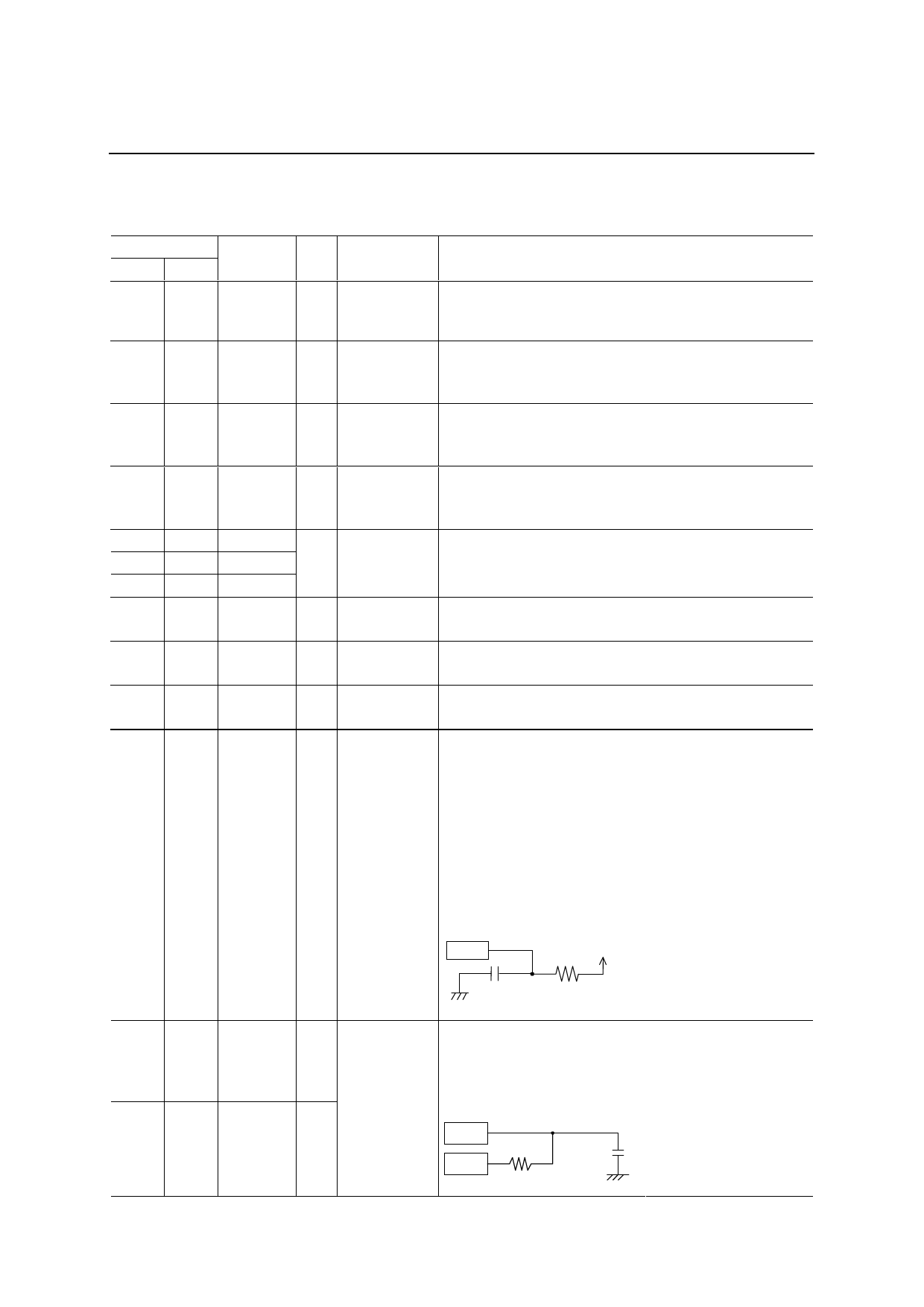
RESET
C2
R2
(Circuit when R and C are
connected externally)
See Application Circuit.
50
58
OSC0
I
51
59
OSC1 O
C1, R1
External RC pin for RC oscillation.
Connect R and C externally. The RC time constant
depends on the VDD voltage used. Set the target oscillation
frequency to 2 MHz.
OSC0
R1
OSC1
(RC oscillation circuit)
C1 See Application Circuit.
5/33
Share Link: