MX29LV161DB Ver la hoja de datos (PDF) - Macronix International
Número de pieza
componentes Descripción
Lista de partido
MX29LV161DB Datasheet PDF : 63 Pages
| |||
MX29LV161D T/B
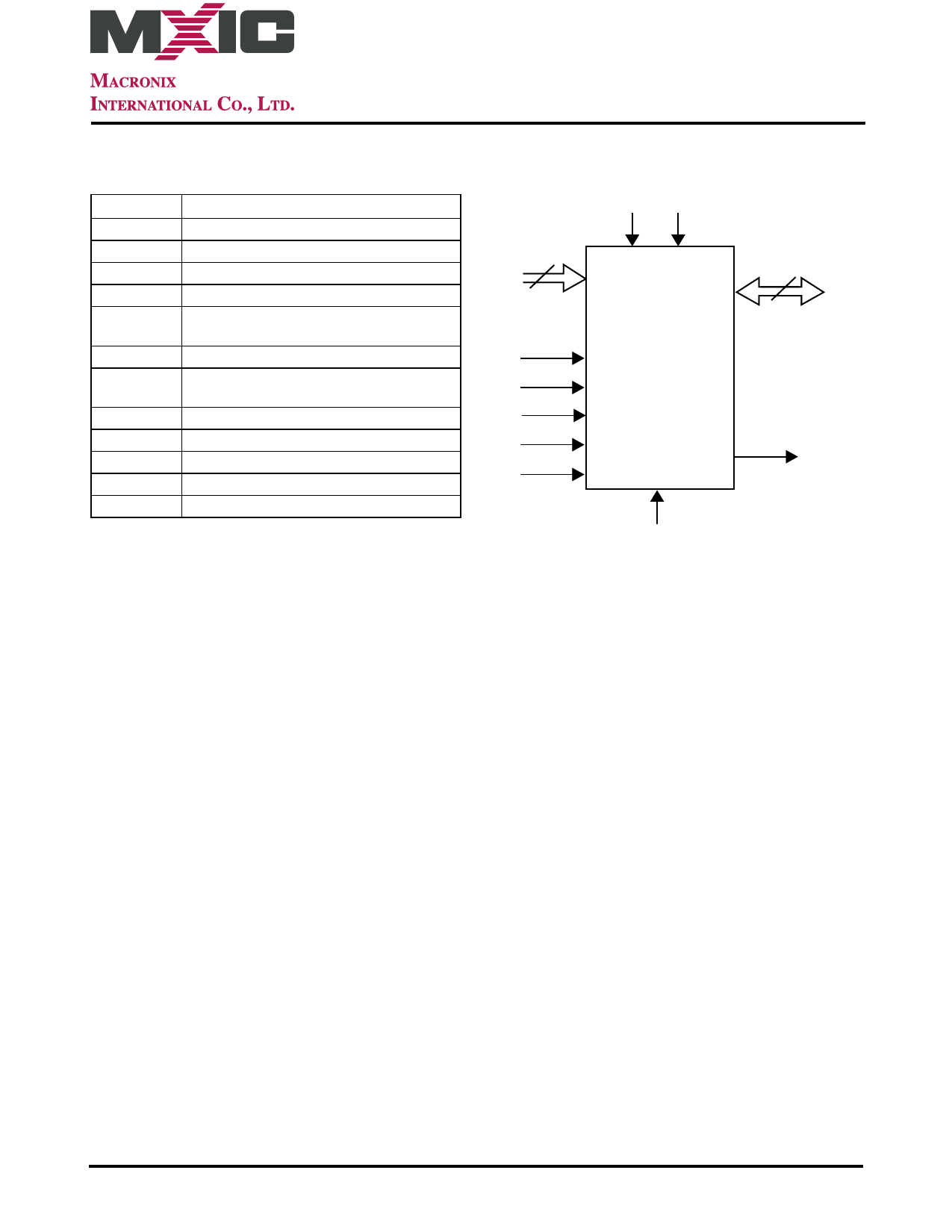
PIN DESCRIPTION
LOGIC SYMBOL
SYMBOL
A0~A19
Q0~Q15
CE#
WE#
RESET#
OE#
PIN NAME
Address Input
Data Input/Output
Chip Enable Input
Write Enable Input
Hardware Reset Pin/Sector Protect
Unlock
Output Enable Input
Vcc VI/O
20
16
A0-A19
Q0-Q15
CE#
RY/BY# Ready/Busy Output
OE#
VCC Power Supply Pin (2.7V~3.6V)
GND Ground Pin
VI/O Power Supply for Input/Output
WP#/ACC Hardware write Protect/Acceleration Pin
NC Pin Not Connected Internally
WE#
RESET#
WP#/ACC
RY/BY#
GND
P/N:PM1359
REV. 1.0, JUN. 03, 2010
9
Share Link: 