82C84A Ver la hoja de datos (PDF) - Renesas Electronics
Número de pieza
componentes Descripción
Lista de partido
82C84A Datasheet PDF : 13 Pages
| |||
82C84A
Absolute Maximum Ratings
Supply Voltage . . . . . . . . . . . . . . . . . . . . . . . . . . . . . . . . . . . . . +8.0V
Input, Output or I/O Voltage . . . . . . . . . . . . GND -0.5V to VCC +0.5V
ESD Classification . . . . . . . . . . . . . . . . . . . . . . . . . . . . . . . . . Class 1
Operating Conditions
Operating Voltage Range. . . . . . . . . . . . . . . . . . . . . . +4.5V to +5.5V
Operating Temperature Range
C82C84A . . . . . . . . . . . . . . . . . . . . . . . . . . . . . . . . . 0oC to +70oC
I82C84A . . . . . . . . . . . . . . . . . . . . . . . . . . . . . . . . -40oC to +85oC
M82C84A . . . . . . . . . . . . . . . . . . . . . . . . . . . . . . -55oC to +125oC
Thermal Information
Thermal Resistance. . . . . . . . . . . . . . . . . JA (oC/W) JC (oC/W)
CERDIP Package. . . . . . . . . . . . . . . . .
80
20
CLCC Package . . . . . . . . . . . . . . . . . .
95
28
PDIP Package* . . . . . . . . . . . . . . . . . .
85
N/A
PLCC Package. . . . . . . . . . . . . . . . . . .
85
N/A
Storage Temperature Range . . . . . . . . . . . . . . . . . -65oC to +150oC
Max Junction Temperature . . . . . . . . . . . . . . . . . . . . . . . . . .+175oC
Lead Temperature (Soldering 10s) . . . . . . . . . . . . . . . . . . . .+300oC
(PLCC - Lead Tips Only)
*Pb-free PDIPs can be used for through hole wave solder processing
only. They are not intended for use in Reflow solder processing
applications.
Die Characteristics
Gate Count . . . . . . . . . . . . . . . . . . . . . . . . . . . . . . . . . . . . .50 Gates
CAUTION: Stresses above those listed in “Absolute Maximum Ratings” may cause permanent damage to the device. This is a stress only rating and operation of the
device at these or any other conditions above those indicated in the operational sections of this specification is not implied.
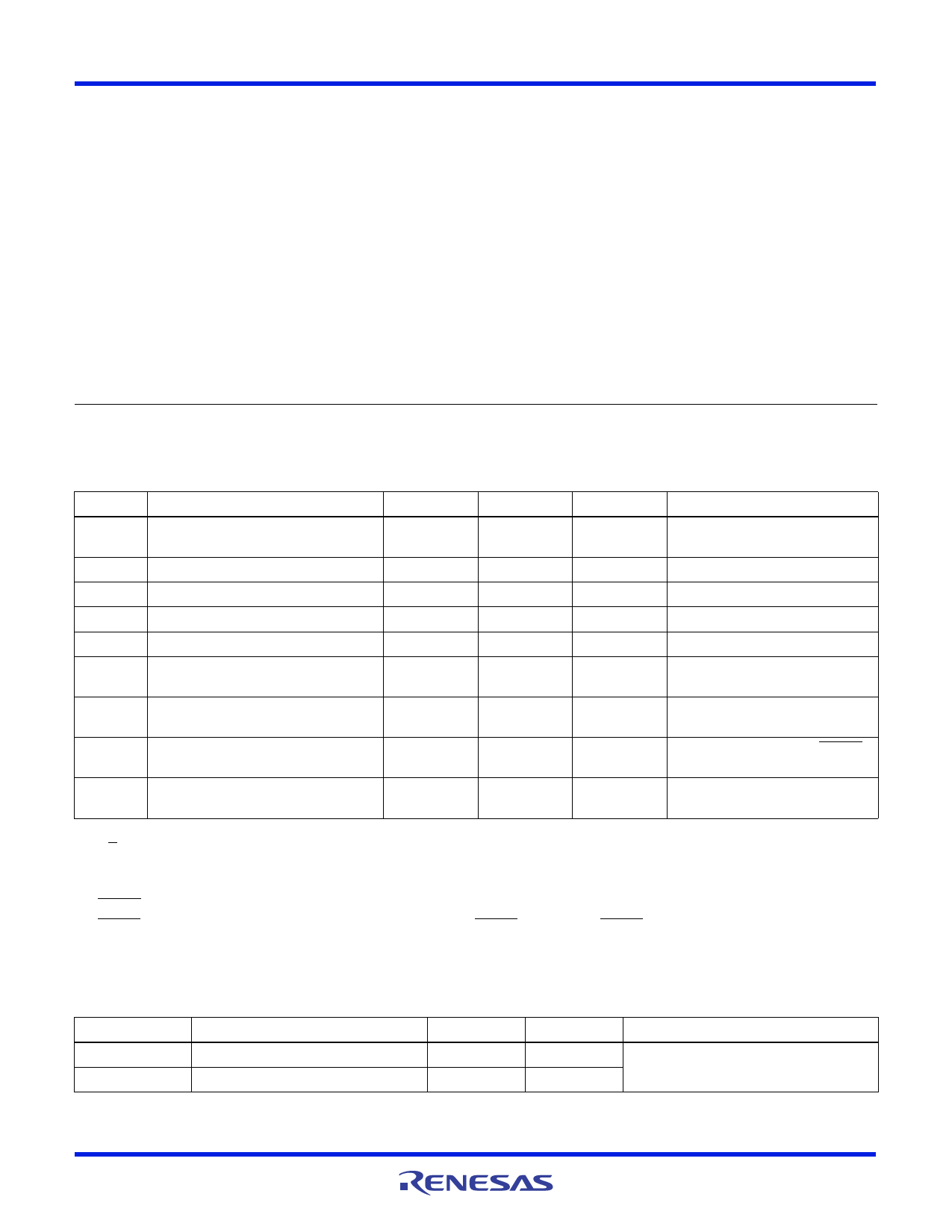
DC Electrical Specifications VCC = +5.0V10%,
TA = 0oC to +70oC (C82C84A),
TA = -40oC to +85oC (I82C84A),
TA = -55oC to +125oC (M82C84A)
SYMBOL
PARAMETER
MIN
MAX
UNITS
TEST CONDITIONS
VIH
Logical One Input Voltage
2.0
-
2.2
V
C82C84A, I82C84
V
M82C84A, Notes 1, 2
VIL
VIHR
VILR
VT+ - VT-
Logical Zero Input Voltage
Reset Input High Voltage
Reset Input Low Voltage
Reset Input Hysteresis
VOH Logical One Output Current
VOL
Logical Zero Output Voltage
II
Input Leakage Current
-
0.8
VCC -0.8
-
-
0.5
0.2 VCC
-
VCC -0.4
-
-
0.4
-1.0
1.0
V
Notes 1, 2, 3
V
V
-
V
IOH = -4.0mA for CLK Output
IOH = -2.5mA for All Others
V
IOL = +4.0mA for CLK Output
IOL = +2.5mA for All Others
A
VIN = VCC or GND except ASYNC,
X1: (Note 4)
ICCOP Operating Power Supply Current
-
40
mA
Crystal Frequency = 25MHz
Outputs Open, Note 5
NOTES:
1. F/C is a strap option and should be held either 0.8V or 2.2V. Does not apply to X1 or X2 pins.
2. Due to test equipment limitations related to noise, the actual tested value may differ from that specified, but the specified limit is
guaranteed.
3. CSYNC pin is tested with VIL 0.8V.
4. ASYNC pin includes an internal 17.5k nominal pull-up resistor. For ASYNC input at GND, ASYNC input leakage current = 300A
nominal, X1 - crystal feedback input.
5. f = 25MHz may be tested using the extrapolated value based on measurements taken at f = 2MHz and f = 10MHz.
Capacitance TA = +25oC
SYMBOL
PARAMETER
CIN
COUT
Input Capacitance
Output Capacitance
TYPICAL
10
15
UNITS
pF
pF
TEST CONDITIONS
FREQ = 1MHz, all measurements are
referenced to device GND
FN2974 Rev 4.00
Sep 9, 2015
Page 7 of 13
Share Link: 