CY23S08SXI-4T(2007) Ver la hoja de datos (PDF) - Cypress Semiconductor
Número de pieza
componentes Descripción
Lista de partido
CY23S08SXI-4T Datasheet PDF : 10 Pages
| |||
Pinouts
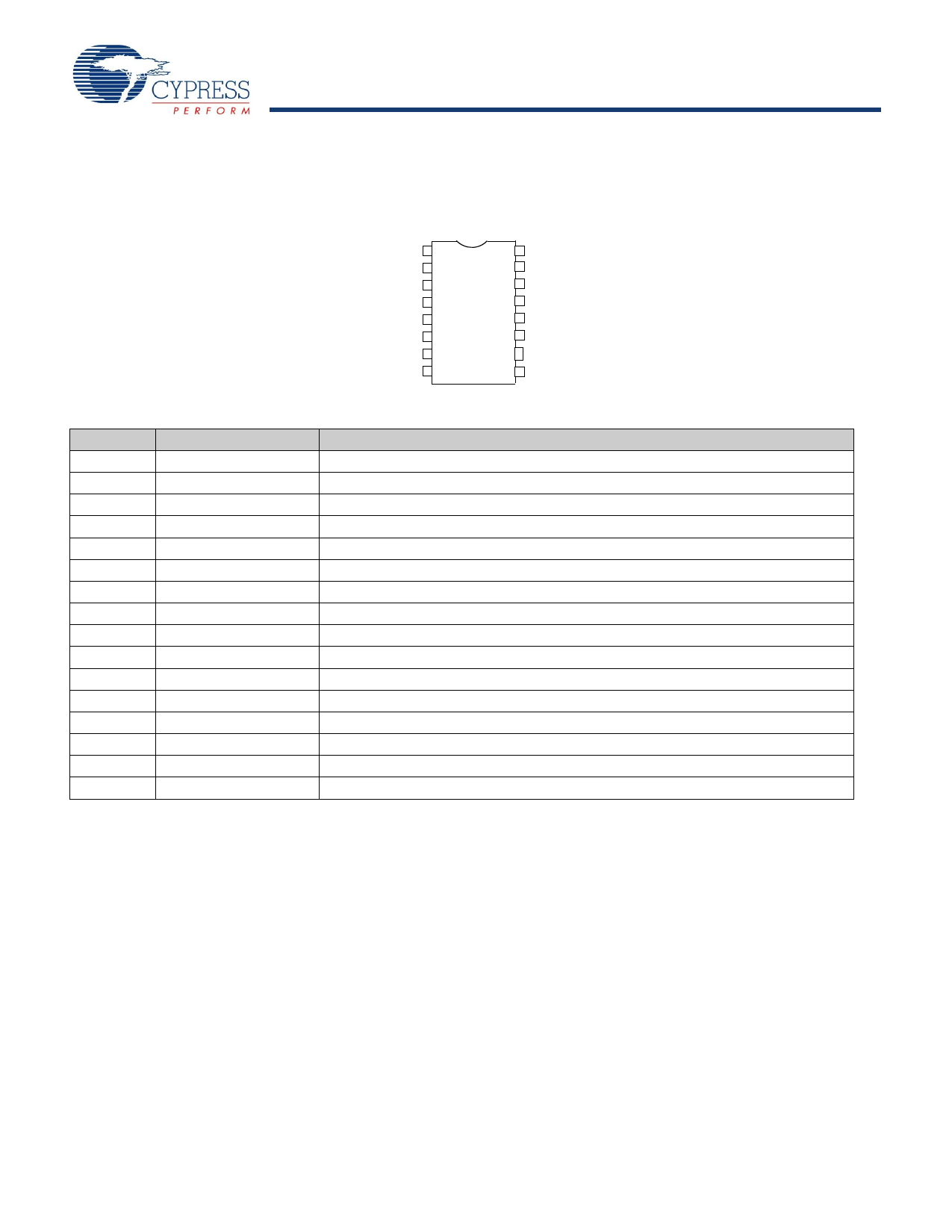
Figure 1. Pin Diagram - 16 Pin SOIC Package
REF
CLKA1
CLKA2
VDD
GND
CLKB1
CLKB2
S2
Top View
1
16
2
15
3
14
4 SOIC 13
5
12
6
11
7
10
8
9
FBK
CLKA4
CLKA3
VDD
GND
CLKB4
CLKB3
S1
Table 1. Pin Definition - 16 Pin SOIC Package
Pin
Signal
Description
1
REF[2]
Input reference frequency, 5V tolerant input
2
CLKA1[3]
Clock output, Bank A
3
CLKA2[3]
Clock output, Bank A
4
VDD
5
GND
6
CLKB1[3]
7
CLKB2[3]
8
S2[4]
9
S1[4]
10
CLKB3[3]
11
CLKB4[3]
3.3V supply
Ground
Clock output, Bank B
Clock output, Bank B
Select input, bit 2
Select input, bit 1
Clock output, Bank B
Clock output, Bank B
12
GND
Ground
13
VDD
14
CLKA3[3]
15
CLKA4[3]
3.3V supply
Clock output, Bank A
Clock output, Bank A
16
FBK
PLL feedback input
CY23S08
Notes
1. Output phase is indeterminant (0° or 180° from input clock). If phase integrity is required, use the CY23S08–2.
2. Weak pull down.
3. Weak pull down on all outputs.
4. Weak pull ups on these inputs.
Document #: 38-07265 Rev. *G
Page 2 of 10
[+] Feedback
Share Link: 