MAX8631XEVKIT Ver la hoja de datos (PDF) - Maxim Integrated
Número de pieza
componentes Descripción
Lista de partido
MAX8631XEVKIT Datasheet PDF : 8 Pages
| |||
MAX8631X Evaluation Kit
Shutdown Control
One jumper is included on the EV kit for shutting down
the main LEDs. To turn off the main LEDs, place the
shunt on the OFF side of jumper JU5 (pins 2-3). Note
that with JU5 shunted off, power is disconnected from
the pulse-generator circuit. The MAX8631X is in low-
power shutdown mode when both JU5 and JU3 are
shunted off since flash is nominally off (see the Low-
Dropout (LDO) Regulator section).
Changing the Number of LEDs
The EV kit comes with four LEDs for the main display
and a flash LED module. To use fewer LEDs, locate the
small pad (labeled TP_) next to the LED to be removed
and connect it to the pad on the EV kit labeled TP9.
Connecting External LEDs
To connect external LEDs to the MAX8631X EV kit, cut
the trace shorting JU7. Connect the anodes of all the
external LEDs to the small pad labeled TP9. Connect
the cathodes to the small pads next to D1–D8
(TP1–TP4 for the main LEDs, TP5–TP8 for the flash
LEDs). Connect any unused pads (TP1–TP8) to the pad
labeled TP9. Also, cut JU8 and JU9 as needed to sup-
port individual flash LEDs.
Low-Dropout (LDO) Regulator
LDO Shutdown
One jumper is included on the EV kit for shutting down
both LDOs. To turn off the LDOs, place the shunt on the
OFF side (pins 2-3) of jumper JU3. To turn on the
LDOs, place the shunt on the ON side (pins 1-2) of
jumper JU3.
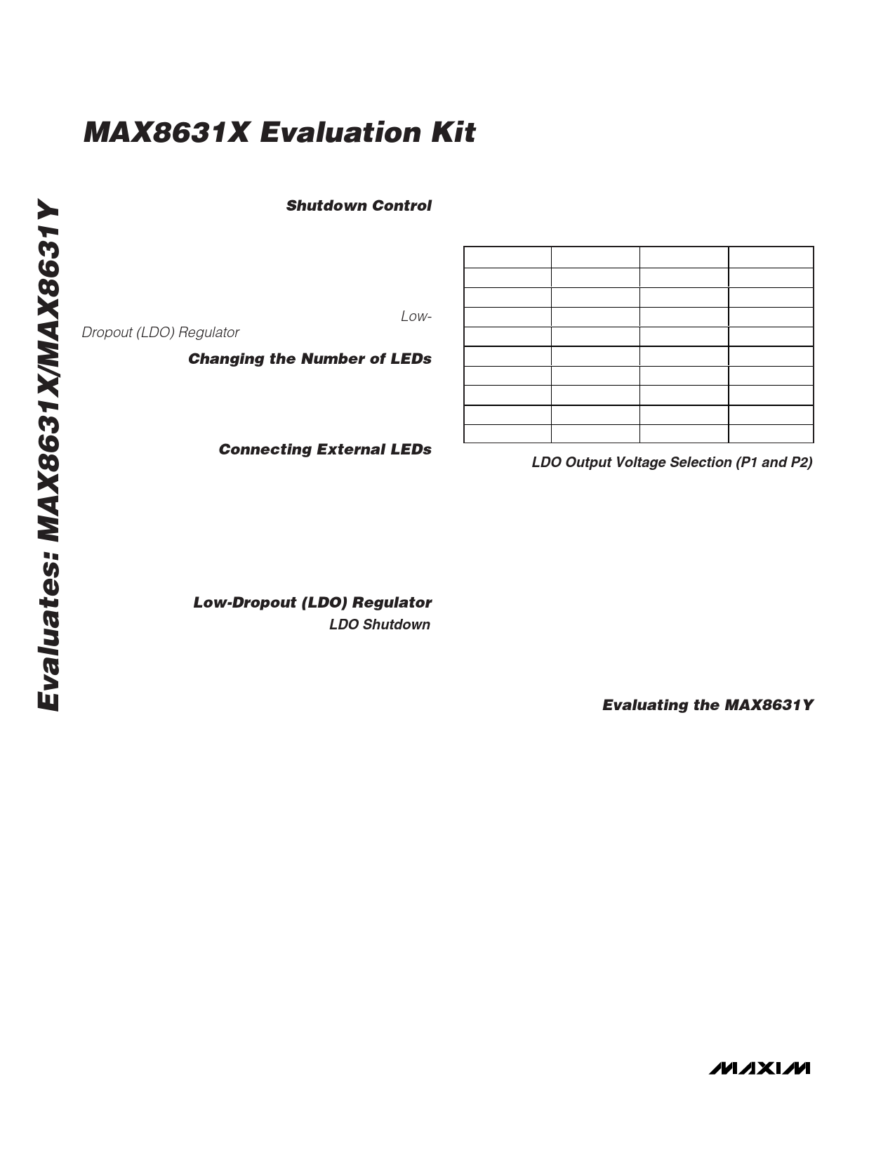
Table 1. P1 and P2, LDO Output Voltage
Selection for MAX8631X
P1
GND
GND
GND
IN
IN
IN
OPEN
OPEN
OPEN
P2
GND
OPEN
IN
GND
OPEN
IN
GND
OPEN
IN
LDO1 (V)
2.5
2.8
3.0
2.8
3.0
3.3
2.6
2.6
3.3
LDO2 (V)
1.8
1.8
1.8
1.5
1.5
1.8
1.5
1.8
1.5
LDO Output Voltage Selection (P1 and P2)
As shown in Table 1, the LDO output voltages, LDO1
and LDO2, are pin programmable by the logic states of
P1 (jumper JU1) and P2 (jumper JU2). P1 and P2 are tri-
level inputs: IN (pins 1-2), open, and GND (pins 2-3).
The input voltage, VIN, must be greater than the select-
ed LDO1 and LDO2 output voltages to prevent dropout.
The logic states of P1 and P2 can be programmed only
when ENLDO is low. Once the LDO_ voltages are pro-
grammed, their values do not change by changing P1
or P2 when ENLDO is high.
When evaluating the MAX8631Y, refer to the
MAX8631X/MAX8631Y IC data sheet for the LDO out-
put-voltage selection.
Evaluating the MAX8631Y
For evaluating the MAX8631Y, carefully remove the
MAX8631X (U1) and install the MAX8631Y. All other
components can remain the same.
4 _______________________________________________________________________________________
Share Link: 