TC74LCX16374FT Ver la hoja de datos (PDF) - Toshiba
Número de pieza
componentes Descripción
Lista de partido
TC74LCX16374FT Datasheet PDF : 10 Pages
| |||
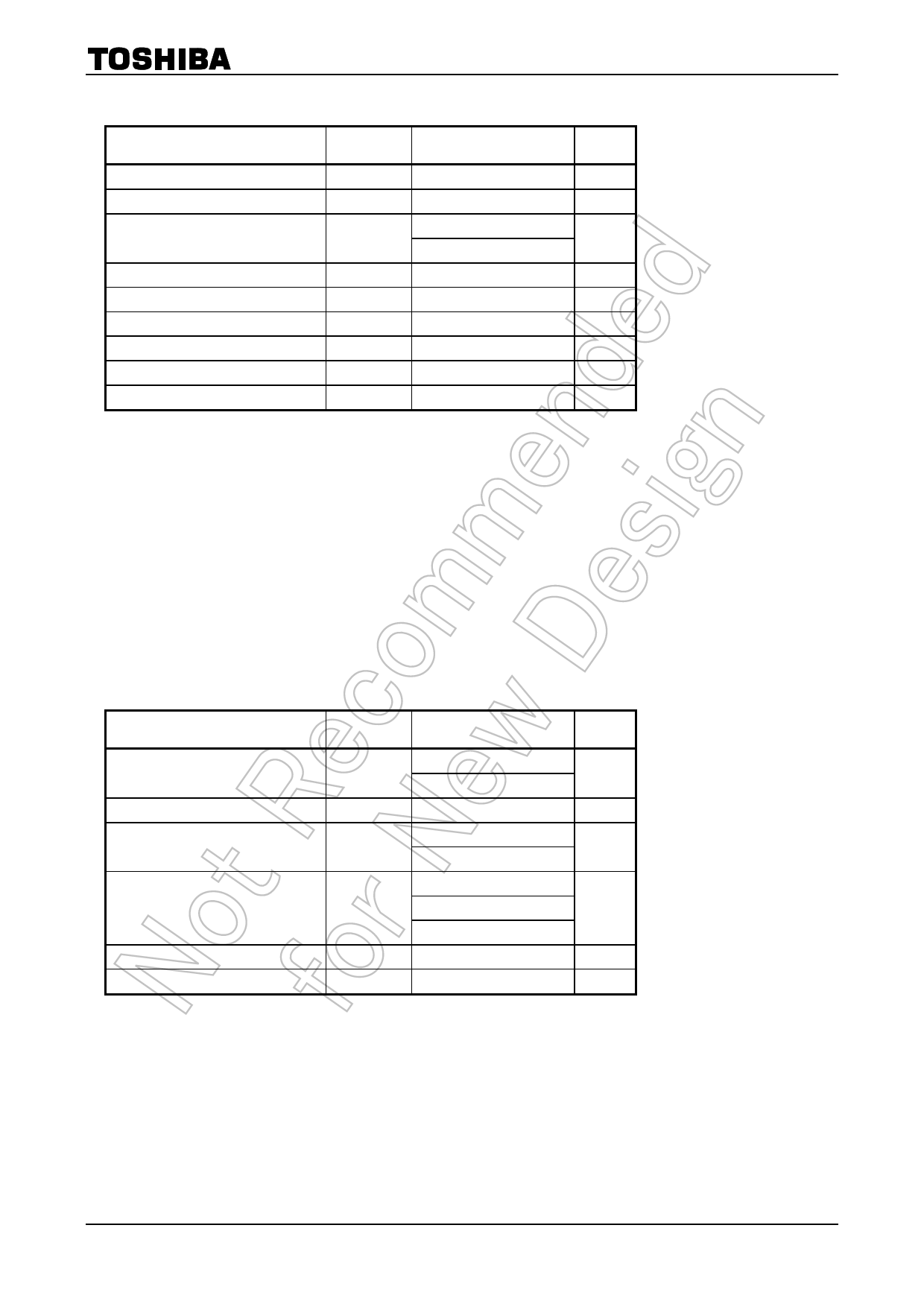
Absolute Maximum Ratings (Note 1)
TC74LCX16374FT
Characteristics
Symbol
Rating
Unit
Power supply voltage
VCC
Input voltage
VIN
Output voltage
VOUT
Input diode current
Output diode current
DC output current
Power dissipation
DC VCC/ground current per supply pin
Storage temperature
IIK
IOK
IOUT
PD
ICC/IGND
Tstg
−0.5 to 6.0
V
−0.5 to 7.0
V
−0.5 to 7.0 (Note 2)
V
−0.5 to VCC + 0.5 (Note 3)
−50
mA
±50 (Note 4) mA
±50
mA
400
mW
±100
mA
−65 to 150
°C
Note 1: Exceeding any of the absolute maximum ratings, even briefly, lead to deterioration in IC performance or
even destruction.
Using continuously under heavy loads (e.g. the application of high temperature/current/voltage and the
significant change in temperature, etc.) may cause this product to decrease in the reliability significantly
even if the operating conditions (i.e. operating temperature/current/voltage, etc.) are within the absolute
maximum ratings and the operating ranges.
Please design the appropriate reliability upon reviewing the Toshiba Semiconductor Reliability Handbook
(“Handling Precautions”/“Derating Concept and Methods”) and individual reliability data (i.e. reliability test
report and estimated failure rate, etc).
Note 2: Output in OFF state
Note 3: High or low state. IOUT absolute maximum rating must be observed.
Note 4: VOUT < GND, VOUT > VCC
Operating Ranges (Note 1)
Characteristics
Symbol
Rating
Unit
Power supply voltage
Input voltage
Output voltage
Output current
Operating temperature
Input rise and fall time
VCC
VIN
VOUT
IOH/IOL
Topr
dt/dv
2.0 to 3.6
1.5 to 3.6 (Note 2)
0 to 5.5
0 to 5.5 (Note 3)
0 to VCC (Note 4)
±24 (Note 5)
±12 (Note 6)
±8 (Note 7)
−40 to 85
0 to 10 (Note 8)
V
V
V
mA
°C
ns/V
Note 1: The operating ranges must be maintained to ensure the normal operation of the device.
Unused inputs must be tied to either VCC or GND.
Note 2: Data retention only
Note 3: Output in OFF state
Note 4: High or low state
Note 5:
Note 6:
Note 7:
Note 8:
VCC = 3.0 to 3.6 V
VCC = 2.7 to 3.0 V
VCC = 2.3 to 2.7 V
VIN = 0.8 to 2.0 V, VCC = 3.0 V
4
2014-03-01
Share Link: 