NCV8664C Ver la hoja de datos (PDF) - ON Semiconductor
Número de pieza
componentes Descripción
Lista de partido
NCV8664C Datasheet PDF : 16 Pages
| |||
NCV8664C
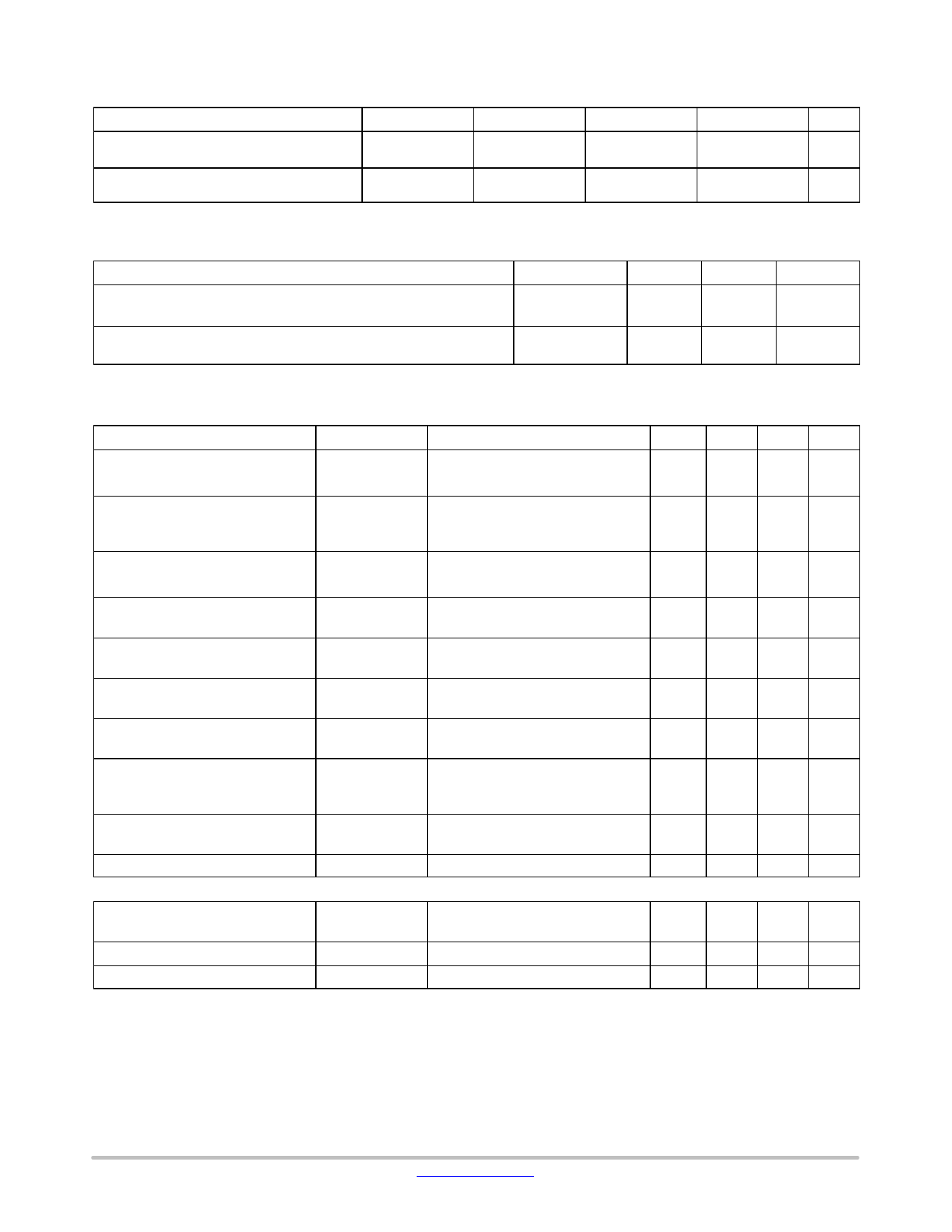
THERMAL RESISTANCE
Parameter
Junction−to−Ambient
DPAK
SOT−223
Junction−to−Tab
DPAK
SOT−223
2. 1 oz copper, 100 mm2 copper area, FR4.
Symbol
RqJA
RyJT
Condition
LEAD SOLDERING TEMPERATURE AND MSL
Rating
Lead Temperature Soldering
Reflow (SMD Styles Only), Lead Free (Note 3)
Moisture Sensitivity Level
SOT223
DPAK
3. Lead Free, 60 sec – 150 sec above 217°C, 40 sec max at peak.
Symbol
Tsld
MSL
Min
−
−
−
−
Min
−
3
1
Max
87.4 (Note 2)
109 (Note 2)
3.5
10.9
Unit
°C/W
°C/W
Max
Unit
°C
265 pk
−
−
−
ELECTRICAL CHARACTERISTICS (VIN = 13.5 V, Tj = −40°C to +150°C, unless otherwise noted.)
Characteristic
Symbol
Test Conditions
Min
Typ Max Unit
Output Voltage
5.0 V Version
Output Voltage
5.0 V Version
Output Voltage
3.3 V Version
Line Regulation
5.0 V Version
Line Regulation
3.3 V Version
Load Regulation
VOUT
VOUT
VOUT
DVOUT vs. VIN
DVOUT vs. VIN
DVOUT vs. IOUT
0.1 mA v IOUT v 150 mA (Note 4)
6.0 V v VIN v 28 V
0 mA v IOUT v 150 mA
5.5 V v VIN v 28 V
−40°C v TJ v 125°C
0.1 mA v IOUT v 150 mA (Note 4)
4.5 V v VIN v 28 V
IOUT = 5.0 mA
6.0 V v VIN v 28 V
IOUT = 5.0 mA
4.5 V v VIN v 28 V
1.0 mA v IOUT v 150 mA
(Note 4)
4.900
4.900
3.234
−25
−25
−35
5.0 5.100 V
5.0 5.100 V
3.3 3.366 V
0.7
+25
mV
0.6
+25
mV
0.5
+35
mV
Dropout Voltage
5.0 V Version
Quiescent Current
Active Ground Current
Power Supply Rejection
VIN−VOUT
Iq
IG(ON)
PSRR
IQ = 100 mA (Notes 4 & 5)
IQ = 150 mA (Notes 4 & 5)
IOUT = 100 mA
TJ = 25°C
TJ = −40°C to +85°C
IOUT = 50 mA (Note 4)
IOUT = 150 mA (Note 4)
VRIPPLE = 0.5 VP−P, F = 100 Hz
−
230 500 mV
−
270 600
mA
−
21
29
−
22
30
−
0.5
3
mA
−
3.1
15
−
67
−
dB
PROTECTION
Current Limit
IOUT(LIM)
VOUT = 4.5 V (5.0 V Version) (Note 4) 150
VOUT = 3.0 V (3.3 V Version) (Note 4) 150
−
500 mA
−
500
Short Circuit Current Limit
IOUT(SC)
VOUT = 0 V (Note 4)
100
−
500 mA
Thermal Shutdown Threshold
TTSD
(Note 6)
150
−
200
°C
Product parametric performance is indicated in the Electrical Characteristics for the listed test conditions, unless otherwise noted. Product
performance may not be indicated by the Electrical Characteristics if operated under different conditions.
4. Use pulse loading to limit power dissipation.
5. Dropout voltage = (VIN – VOUT), measured when the output voltage has dropped 100 mV relative to the nominal value obtained with VIN = 13.5 V.
6. Not tested in production. Limits are guaranteed by design.
www.onsemi.com
3
Share Link: 