LT1944-1 Ver la hoja de datos (PDF) - Linear Technology
Número de pieza
componentes Descripción
Lista de partido
LT1944-1 Datasheet PDF : 8 Pages
| |||
LT1944-1
BLOCK DIAGRA
VIN
C1
8 VIN
L1
SHDN1
2
VOUT1
R1
(EXTERNAL)
R2
(EXTERNAL)
FB1
1
R5
R6
40k
40k
+
–
Q1
Q2
X10
R3
30k
R4
140k
GND
3
A1
ENABLE
400ns
ONE-SHOT
RESET
A2
SWITCHER 1
D1
SW1
10
VOUT1
C2
VOUT2
C3
D2
SW2
6
Q3
DRIVER
Q3B
DRIVER
12mV
0.12Ω
0.12Ω
21mV
PGND PGND
9
7
L2
VIN
SHDN2
4
VIN
R6B R5B
40k 40k
A1B
ENABLE
1.5µs
ONE-SHOT
RESET
A2B
SWITCHER 2
+
–
Q2B
X10
R3B
30k
R4B
140k
VOUT2
Q1B
FB2
5
R1B
(EXTERNAL)
R2B
(EXTERNAL)
1944-1 BD
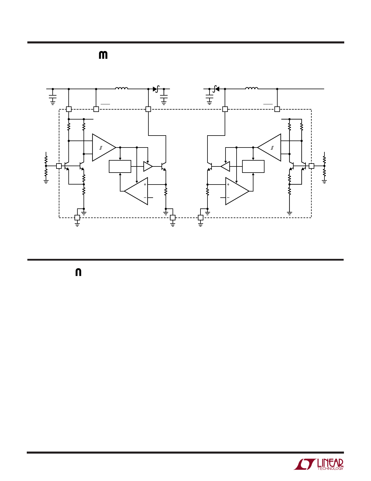
Figure 1. LT1944-1 Block Diagram
U
OPERATIO
The LT1944-1 uses a constant off-time control scheme to
provide high efficiencies over a wide range of output
current. Operation can be best understood by referring to
the block diagram in Figure 1. Q1 and Q2 along with R3 and
R4 form a bandgap reference used to regulate the output
voltage. When the voltage at the FB1 pin is slightly above
1.23V, comparator A1 disables most of the internal cir-
cuitry. Output current is then provided by capacitor C2,
which slowly discharges until the voltage at the FB1 pin
drops below the lower hysteresis point of A1 (typical
hysteresis at the FB pin is 8mV). A1 then enables the
internal circuitry, turns on power switch Q3, and the
current in inductor L1 begins ramping up. Once the switch
current reaches 100mA, comparator A2 resets the one-
shot, which turns off Q3 for 400ns. L1 then delivers
current to the output through diode D1 as the inductor
current ramps down. Q3 turns on again and the inductor
current ramps back up to 100mA, then A2 resets the one-
shot, again allowing L1 to deliver current to the output.
This switching action continues until the output voltage is
charged up (until the FB1 pin reaches 1.23V), then A1
turns off the internal circuitry and the cycle repeats. The
LT1944-1 contains additional circuitry to provide protec-
tion during start-up and under short-circuit conditions.
When the FB1 pin voltage is less than approximately
600mV, the switch off-time is increased to 1.5µs and the
current limit is reduced to around 70mA (70% of its
normal value). This reduces the average inductor current
and helps minimize the power dissipation in the power
switch and in the external inductor and diode.
The second switching regulator operates in the same
manner, but with a 175mA current limit and an off-time of
1.5µs. With this longer off-time, switcher 2 is ideal for very
low duty cycle applications (i.e. Li-Ion to 5V boost
converters).
4
Share Link: 