IR213 Ver la hoja de datos (PDF) - Infineon Technologies
Número de pieza
componentes Descripción
Lista de partido
IR213 Datasheet PDF : 36 Pages
| |||
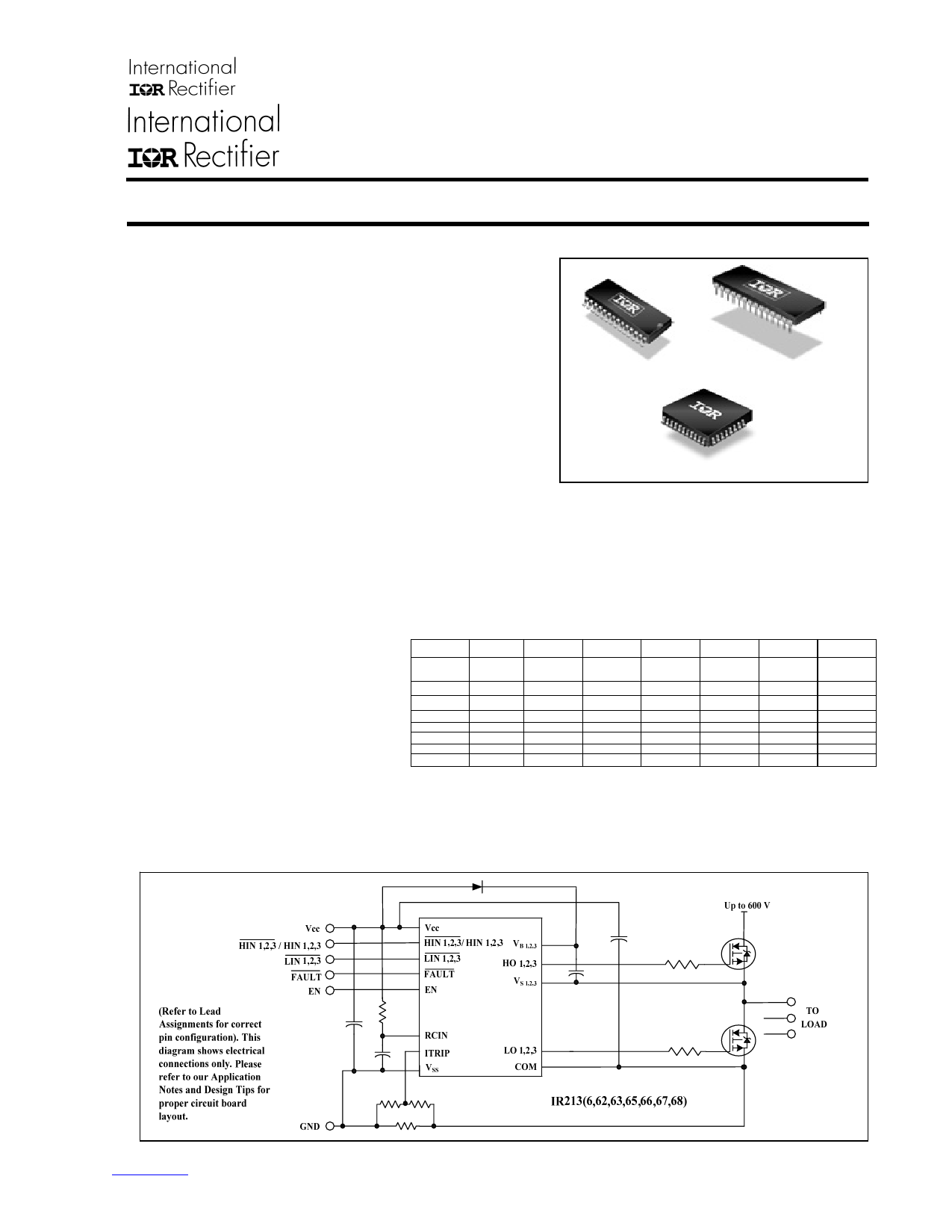
IR213(6,62,63,65,66,67,68)(J&S) & PbF
Data Sheet No. PD60166 revU
IR2136/IR21362/IR21363/IR21365/
IR21366/IR21367/IR21368 (J&S) & (PbF)
600 V three-phase gate driver IC with OCP, Enable, and Fault
Features
• Floating channel designed for bootstrap operation
• Fully operational to +600 V
• Tolerant to negative transient voltage, dV/dt immune
• Gate drive supply range from 10 V to 20 V (IR2136/
IR21368), 11.5 V to 20 V (IR21362D), or 12 V to 20 V
(IR21363/IR21365/IR21366/IR21367)
• Undervoltage lockout for all channels
• Over-current shutdown turns off all six drivers
• Independent 3 half-bridge drivers
• Matched propagation delay for all channels
• Cross-conduction prevention logic
• Low side output out of phase with inputs. High side outputs
out of phase (IR213(6,63, 65, 66, 67, 68)), or in phase
(IR21362) with inputs
• 3.3 V logic compatible
• Lower di/dt gate drive for better noise immunity
• Externally programmable delay for automatic fault clear
• All parts are LEAD-FREE
Packages
28-Lead SOIC
28-Lead PDIP
44-Lead PLCC w/o 12 Leads
Description
Feature Comparison: IR213(6,62,63,65,66,67,68)
The IR2136x (J&S) are high voltage, high
Part
IR2136
IR21362
IR21363
IR21365
IR21366
IR21367
IR21368
speed power MOSFET and IGBT drivers with
three independent high and low side
referenced output channels for 3-phase
applications. Proprietary HVIC technology
enables ruggedized monolithic construction.
Input Logic
Ton (typ.)
Toff (typ.)
VIH (typ.)
VIL (typ.)
___ ___
HIN, LIN
400 ns
380ns
2.7 V
1.7 V
___
HIN, LIN
400 ns
380 ns
2.7 V
1.7 V
___ ___
HIN, LIN
400 ns
380 ns
2.7 V
1.7 V
___ ___
HIN, LIN
400 ns
380 ns
2.7 V
1.7 V
___ ___
HIN, LIN
250 ns
180 ns
2.0 V
1.3 V
___ ___
HIN, LIN
250 ns
180 ns
2.0 V
1.3 V
___ ___
HIN, LIN
400 ns
380 ns
2.0 V
1.3 V
Logic inputs are compatible with CMOS or
Vitrip+
0.46 V
0.46 V
0.46 V
4.3 V
0.46 V
4.3 V
4.3 V
LSTTL outputs, down to 3.3 V logic. A current
UVCC/BS+
UVCC/BS-
8.9 V
8.2 V
10.4 V
9.4 V
11.2 V
11.0 V
11.2 V
11.0 V
11.2 V
11.0 V
11.2 V
11.0 V
8.9 V
8.2 V
trip function which terminates all six outputs
can be derived from an external current sense resistor. An enable function is available to terminate all six outputs simultaneously. An
open-drain FAULT signal is provided to indicate that an overcurrent or undervoltage shutdown has occurred. Overcurrent fault
conditions are cleared automatically after a delay programmed externally via an RC network connected to the RCIN input. The output
drivers feature a high pulse current buffer stage designed for minimum driver cross-conduction. Propagation delays are matched to
simplify use in high frequency applications. The floating channels can be used to drive N-channel power MOSFETs or IGBTs in the
high side configuration which operates up to 600 V.
Typical Connection
www.irf.com
1
Share Link: 