UPC8120T Ver la hoja de datos (PDF) - NEC => Renesas Technology
Número de pieza
componentes Descripción
Lista de partido
UPC8120T
NEC => Renesas Technology

UPC8120T Datasheet PDF : 52 Pages
| |||
µPC8119T, µPC8120T
PIN EXPLANATION
Applied
Pin
Pin Name Voltage
No.
V
1
IN
–
Pin
Voltage
Note
V
1.2
2
GND
0
–
3
4
OUT
Voltage
–
as same
as VCC
through
external
inductor
5
VCC
2.7 to 3.3
–
6
VAGC
0 to 3.3
–
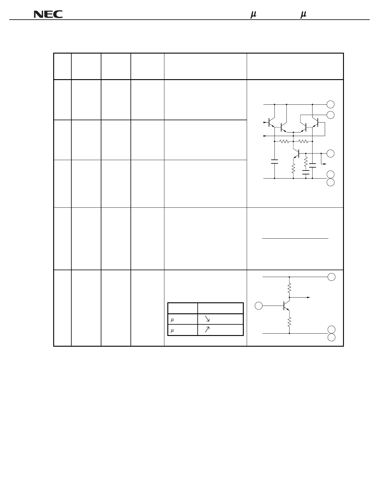
Function and Applications
Internal Equivalent Circuit
RF input pin. This pin should be
coupled with capacitor (eg 1000
pF) for DC cut. This pin can be
input from 50 Ω impedance signal
source without matching circuit.
Ground pin. This pin should be
connected to system ground with
minimum inductance. Ground
pattern on the board should be
formed as wide as possible.
RF output pin. This pin is
designed as open collector of
high impedance.
This pin must be externally
equipped with matching circuits.
Control
circuit
5
4
1
Bias
circuit
2
3
Supply voltage pin. This pin must
be externally equipped with low
pass filter (eg π type) in order to
suppress leakage from input pin.
This pin also must be equipped
with bypass capacitor (eg 1000
pF) to minimize ground
impedance.
Gain control pin. The relation
between product number and
control performance is shown
below;
Part No. VAGC up vs. Gain
6
µPC8119T
down
µPC8120T
up
5
Control
circuit
2
3
Note Pin voltage is measured at VCC = 3.0 V.
3
Share Link: