FAN5234 Ver la hoja de datos (PDF) - Fairchild Semiconductor
Número de pieza
componentes Descripción
Lista de partido
FAN5234 Datasheet PDF : 15 Pages
| |||
FAN5234
PRODUCT SPECIFICATION
Assuming switching losses are about the same for both the
rising edge and falling edge, Q1's switching losses, occur
during the shaded time when the MOSFET has voltage
across it and current through it.
These losses are given by:
PUPPER = PSW + PCOND where:
PSW
=
V-----D----S----×-----I--L-
2
×
2
×
tS
FSW
(15a)
PCOND
=
V---V--O---I-U-N---T-
× IOUT2 × RDS(ON)
(15b)
PUPPER is the upper MOSFET's total losses, and PSW and
PCOND are the switching and conduction losses for a given
MOSFET. RDS(ON) is at the maximum junction temperature
(TJ). tS is the switching period (rise or fall time) and is t2+t3
(Figure 8).
The driver’s impedance and CISS determine t2 while t3’s
period is controlled by the driver's impedance and QGD.
Since most of tS occurs when VGS = VSP we can use a
constant current assumption for the driver to simplify the
calculation of tS:
VDS
C ISS
C RSS
C ISS
tS
=
-Q-----G----(--S---W----)- ≈ -----------------Q-----G----(--S---W----)-----------------
IDRIVER
-R----D---R--V--I--VC----E-C--R---–-+----V-R---S--G-P--A----T---E-
(16)
Most MOSFET vendors specify QGD and QGS. QG(SW) can
be determined as: QG(SW) = QGD + QGS – QTH where QTH is
the gate charge required to get the MOSFET to it's threshold
(VTH). For the high-side MOSFET, VDS = VIN, which can
be as high as 20V in a typical portable application. Care
should also be taken to include the delivery of the
MOSFET's gate power (PGATE ) in calculating the power
dissipation required for the FAN5234:
PGATE = QG × VCC × FSW
(17)
where QG is the total gate charge to reach VCC.
Low-Side Losses
Q2, however, switches on or off with its parallel shottky
diode conducting, therefore VDS ≈ 0.5V. Since PSW is pro-
portional to VDS , Q2's switching losses are negligible and
we can select Q2 based on RDS(ON) only.
Conduction losses for Q2 are given by::
PCOND
=
(1
–
D)
×
IO
U
2
T
×
RDS(ON)
(18)
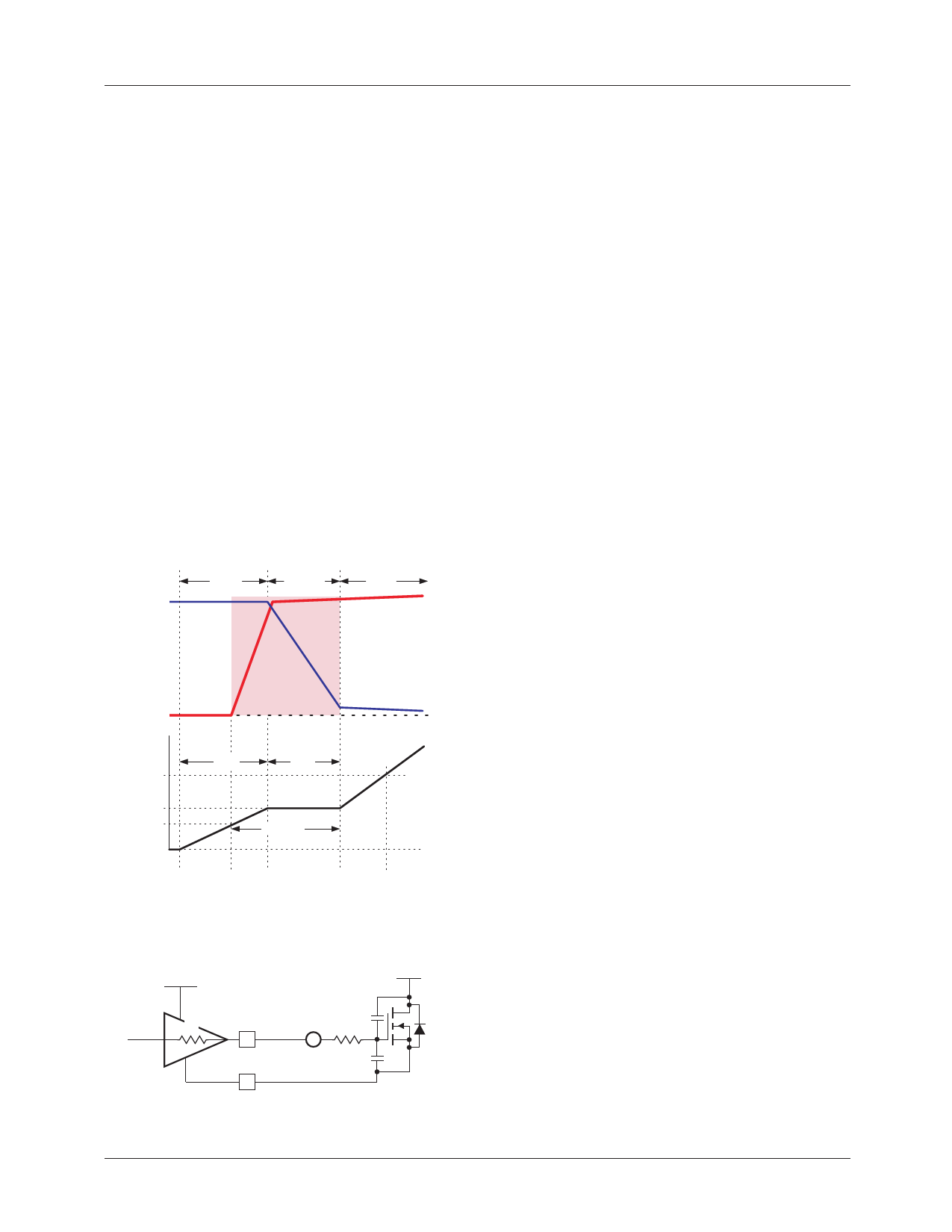
ID
VGS
VSP
VTH
QGS
QGD
QG(SW)
4.5V
t1
t2
CISS = CGS || CGD
t3
t4
t5
Figure 8. Switching losses and QG
5V
RD
VIN
HDRV
SW
C GD
RGATE
G
CGS
where RDS(ON) is the RDS(ON) of the MOSFET at the highest
operating junction temperature and
D
=
V-----O----U----T-
VIN
is the minimum duty cycle for the converter.
Since DMIN < 20% for portable computers, (1-D) ≈ 1
produces a conservative result, further simplifying the
calculation.
The maximum power dissipation (PD(MAX)) is a function of
the maximum allowable die temperature of the low-side
MOSFET, the θJ-A, and the maximum allowable ambient
temperature rise:
PD(MAX) = T----J---(-M-----A----X--θ-)---J–--–---T-A---A----(--M----A----X---)
(19)
θJ-A, depends primarily on the amount of PCB area that can
be devoted to heat sinking (see FSC app note AN-1029 for
SO-8 MOSFET thermal information).
Figure 9. Drive Equivalent Circuitt
REV. 1.0.10 5/3/04
11
Share Link: 