ICS9120M-47 Ver la hoja de datos (PDF) - Integrated Circuit Systems
Número de pieza
componentes Descripción
Lista de partido
ICS9120M-47 Datasheet PDF : 5 Pages
| |||
ICS9120-47
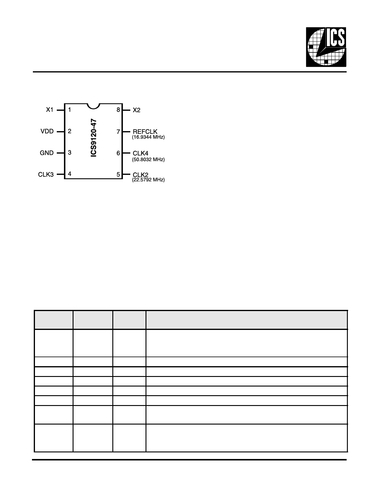
Pin Configuration
8-Pin SOIC
External Components/Crystal Selection
The ICS9120-47 incorporates a crystal oscillator circuit de-signed
to provide 50% duty cycle over a range of operating conditions,
including the addition of external crystal load ca-pacitors to pins
X1 and X2.
For the crystal oscillator, the crystal load capacitance must be
connected externally by adding a capacitor from each of the X1
and X2 pins to ground. A parallel resonant 16.9344 MHz crystal is
recommended.
Duty cycle is also maintained when using an external clock source
(connected to X1, X2 left unconnected) as long as the external
clock has good duty cycle.
Pin Descriptions for ICS9120-47
PIN
PIN NAME
NUMBER
1
X1
2
VDD
3
GND
4
CLK3
5
CLK2
6
CLK4
7
REFCLK
8
X2
TYPE
DESCRIPTION
Input
Power
Power
Output
Output
Output
Output
Output
Crystal or external clock source. Has feedback bias for crystal.
Nominally 16.9344 MHz input applied. (No internal load cap; must
connect external load cap to ground for crystal oscillator).
+Power supply input.
Ground return for Pin 2.
33.8688 MHz target output clock (with nominal 16.9344 MHz input).
22.5792 MHz target output clock (with nominal 16.9344 MHz input).
50.8032 MHz target output clock (with nominal 16.9344 MHz input).
16.9344 MHz reference clock buffered output (with nominal 16.9344
MHz input).
Crystal output drive (leave this pin unconnected when using an
external clock). (No internal load cap; must connect external load cap
to ground for crystal oscillator).
2
Share Link: 