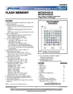
MT28F642D18FN-704BET Hoja de datos - Micron Technology
GENERAL DESCRIPTION
The MT28F642D20 and MT28F642D18 are highperformance, high-density, nonvolatile memory solutions that can significantly improve system performance. This new architecture features a twomemory-bank configuration that supports dual-bank operation with no latency.
FEATURES
• Single device supports asynchronous, page, and burst operations
• Flexible dual-bank architecture
Support for true concurrent operation with zero latency
Read bank a during program bank b and vice versa
Read bank a during erase bank b and vice versa
• Basic configuration:
One hundred and thirty-five erasable blocks
Bank a (16Mb for data storage)
Bank b (48Mb for program storage)
• VCC, VCCQ, VPP voltages
1.70V (MIN), 1.90V (MAX) VCC, VCCQ (MT28F642D18 only)
1.80V (MIN), 2.20V (MAX) VCC, and 2.25V (MAX) VCCQ (MT28F642D20 only)
1.80V (TYP) VPP (in-system PROGRAM/ERASE)
12V ±5% (HV) VPP tolerant (factory programming compatibility)
• Random access time: 70ns @ 1.80V VCC1
• Burst Mode read access
MAX clock rate: 54 MHz (tCLK = 18.5ns)
Burst latency: 70ns @ 1.80V VCC and 54 MHz
tACLK: 15ns @ 1.80V VCC and 54 MHz
• Page Mode read access1
Four-/eight-word page
Interpage read access: 70ns @ 1.80V
Intrapage read access: 30ns @ 1.80V
• Low power consumption (VCC = 2.20V)
Asynchronous Read < 15mA
Interpage Read < 15mA
Intrapage Read < 5mA
Continuous Burst Read < 10mA
WRITE < 55mA (MAX)
ERASE < 45mA (MAX)
Standby < 50µA (MAX)
Automatic power save (APS) feature
Deep power-down < 25µA (MAX)
• Enhanced write and erase suspend options
• Accelerated programming algorithm (APA) insystem and in-factory
• Dual 64-bit chip protection registers for security purposes
• Cross-compatible command support
Extended command set
Common flash interface
• PROGRAM/ERASE cycle
100,000 WRITE/ERASE cycles per block
