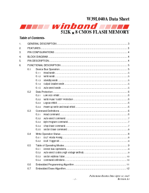
W39L040A Hoja de datos - Winbond
GENERAL DESCRIPTION
The W39L040A is a 4Mbit, 3V/3.3V CMOS flash memory organized as 512K × 8 bits. For flexible erase capability, the 4Mbits of data are divided into 8 uniform sectors of 64 Kbytes. The byte-wide (× 8) data appears on DQ7 − DQ0. The device can be programmed and erased in-system with a standard 3.3V power supply. A 12-volt VPP is not required. The unique cell architecture of the W39L040A results in fast program/erase operations with extremely low current consumption (compared to other comparable 3.3-volt flash memory products). The device can also be programmed and erased by using standard EPROM programmers.
FEATURES
• 3V/3.3-Volt Read/Erase/Program Operations
− 3.0 ~ 3.6V for 70nS
− 2.7 ~ 3.6V for 90nS
• Fast Program operation:
− Byte-by-Byte programming: 9 μS (typ.)
• Fast Erase operation:
− Chip Erase cycle time: 6 S (typ.)
− Sector Erase cycle time: 0.7 S (typ.)
• Read access time: 70/90 nS
• 8 Even sectors with 64K bytes
• Any individual sector can be erased
• Typical program/erase cycles: 10K
• Twenty-year data retention
• Low power consumption
− Active read current: 7 mA at 5MHz (typ.)
− Active program/erase current: 15 mA at
5MHz (typ.)
− Standby current: 0.2 μA (typ.)
• End of program detection
− Software method: Toggle bit/#Data polling
• JEDEC standard byte-wide pinouts
• Available packages: 32-pin PLCC Lead free,
32-pin STSOP (8 x 14 mm) Lead free, 32-pin
PDIP and 32-pin TSOP (8 x 20 mm)
