74ABT543 Ver la hoja de datos (PDF) - Fairchild Semiconductor
Número de pieza
componentes Descripción
Lista de partido
74ABT543 Datasheet PDF : 8 Pages
| |||
Absolute Maximum Ratings(Note 1)
Storage Temperature
−65°C to +150°C
Ambient Temperature under Bias
−55°C to +125°C
Junction Temperature under Bias
−55°C to +150°C
VCC Pin Potential to
Ground Pin
−0.5V to +7.0V
Input Voltage (Note 2)
−0.5V to +7.0V
Input Current (Note 2)
−30 mA to +5.0 mA
Voltage Applied to Any Output
in the Disable or Power-Off State
−0.5V to +5.5V
in the HIGH State
Current Applied to Output
−0.5V to VCC
in LOW State (Max)
twice the rated IOL (mA)
DC Latchup Source Current
Over Voltage Latchup (I/O)
−500 mA
10V
Recommended Operating
Conditions
Free Air Ambient Temperature
−40°C to +85°C
Supply Voltage
+4.5V to +5.5V
Minimum Input Edge Rate (∆V/∆t)
Data Input
50 mV/ns
Enable Input
20 mV/ns
Clock Input
100 mV/ns
Note 1: Absolute maximum ratings are values beyond which the device
may be damaged or have its useful life impaired. Functional operation
under these conditions is not implied.
Note 2: Either voltage limit or current limit is sufficient to protect inputs.
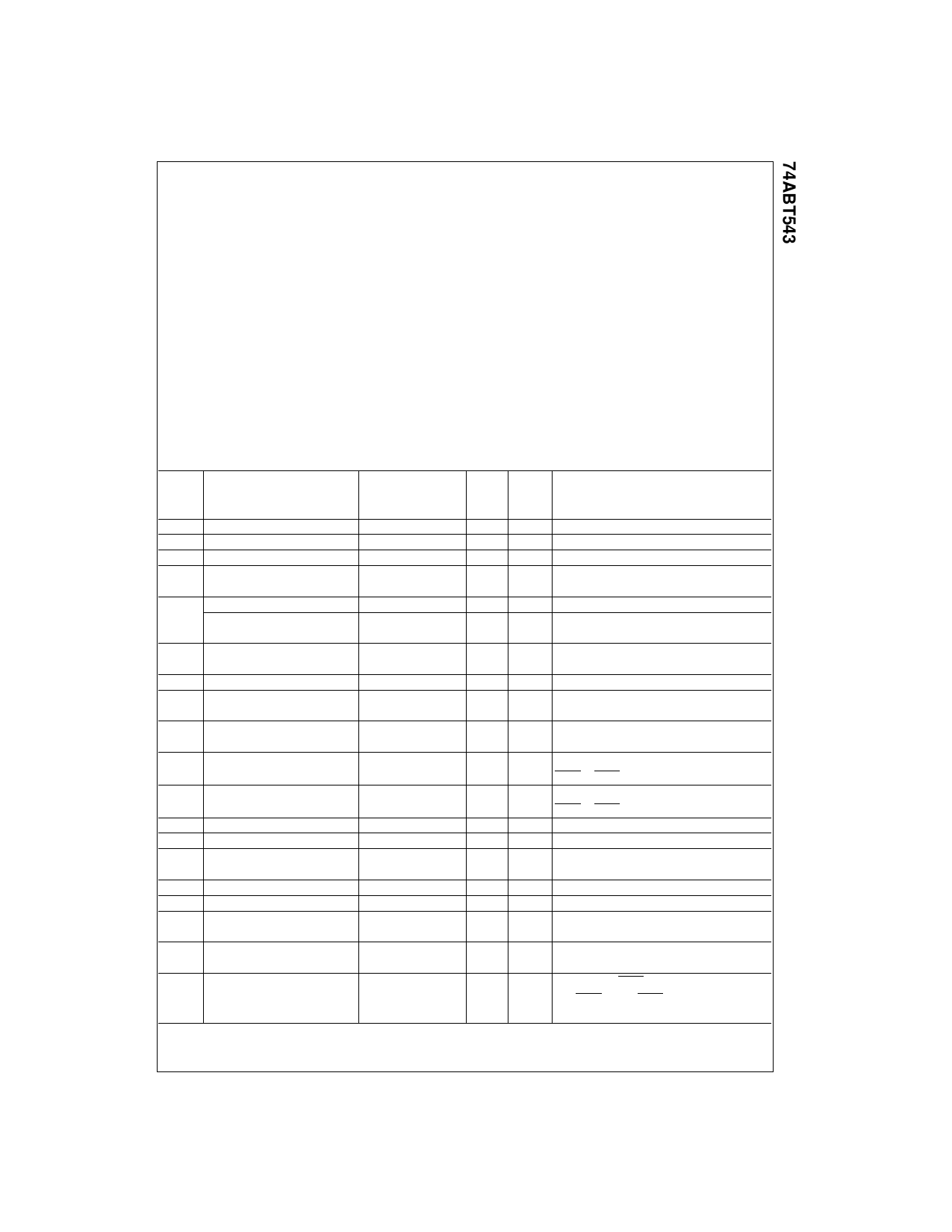
DC Electrical Characteristics
Symbol
Parameter
Min Typ Max Units
VCC
Conditions
VIH
Input HIGH Voltage
VIL
Input LOW Voltage
VCD
Input Clamp Diode Voltage
VOH
Output HIGH Voltage
VOL
Output LOW Voltage
VID
Input Leakage Test
2.0
0.8
2.5
2.0
4.75
IIH
Input HIGH Current
IBVI
IBVIT
IIL
Input HIGH Current Breakdown Test
Input HIGH Current
Breakdown Test (I/O)
Input LOW Current
IIH + IOZH Output Leakage Current
IIL + IOZL Output Leakage Current
IOS
Output Short-Circuit Current
ICEX
Output HIGH Leakage Current
IZZ
Bus Drainage Test
−100
ICCLH
ICCL
ICCZ
Power Supply Current
Power Supply Current
Power Supply Current
ICCT
Additional ICC/Input
ICCD
Dynamic ICC
(Note 5)
No Load
Note 3: Guaranteed but not tested.
Note 4: For 8-bit toggling. ICCD < 1.4 mA/MHz.
Note 5: Guaranteed, but not tested.
V
V
−1.2
V
0.55
V
V
1
µA
1
7
µA
100
µA
Recognized HIGH Signal
Recognized LOW Signal
IIN = −18 mA (Non I/O Pins)
IOH = −3 mA, (An, Bn)
IOH = −32 mA, (An, Bn)
Min IOL = 64 mA, (An, Bn)
0.0 IID = 1.9 µA, (Non-I/O Pins)
All Other Pins Grounded
Max VIN = 2.7V (Non-I/O Pins) (Note 3)
VIN = VCC (Non-I/O Pins)
Max VIN = 7.0V (Non-I/O Pins)
Max VIN = 5.5V (An, Bn)
−1
−1
10
−10
−275
50
100
50
30
50
2.5
0.18
µA
Max VIN = 0.5V (Non-I/O Pins) (Note 3)
VIN = 0.0V (Non-I/O Pins)
µA 0V–5.5V VOUT = 2.7V (An, Bn);
OEAB or CEAB = 2V
µA 0V–5.5V VOUT = 0.5V (An, Bn);
OEAB or CEAB = 2V
mA
Max VOUT = 0V (An, Bn)
µA
Max VOUT = VCC (An, Bn)
µA
0.0V VOUT = 5.5V (An, Bn);
All Others GND
µA
Max All Outputs HIGH
mA
Max All Outputs LOW
µA
Max Outputs 3-STATE
All Others at VCC or GND
mA
Max VI = VCC − 2.1V
All Others at VCC or GND
Outputs Open, CEAB
mA/MHz Max and OEAB = GND, CEBA = VCC, One Bit Toggling,
50% Duty Cycle, (Note 4)
3
www.fairchildsemi.com
Share Link: 