74ABT543 Ver la hoja de datos (PDF) - Fairchild Semiconductor
Número de pieza
componentes Descripción
Lista de partido
74ABT543 Datasheet PDF : 8 Pages
| |||
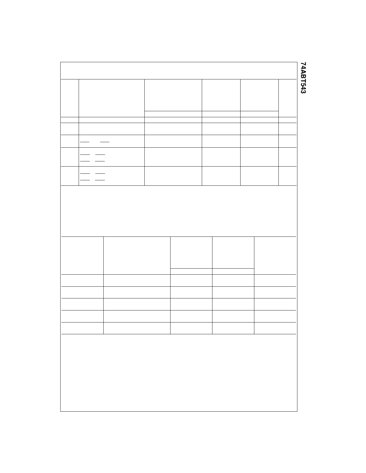
Extended AC Electrical Characteristics
(SOIC Package)
TA = −40°C to +85°C
TA = −40°C to +85°C TA = −40°C to +85°C
VCC = 4.5V–5.5V
VCC = 4.5V–5.5V
VCC = 4.5V–5.5V
Symbol
Parameter
CL = 50 pF
8 Outputs Switching
CL = 250 pF
CL = 250 pF
1 Output Switching 8 Outputs Switching
Units
(Note 9)
(Note 10)
(Note 11)
Min
Typ
Max
Min
Max
Min
Max
fTOGGLE Max Toggle Frequency
100
MHz
tPLH
Propagation Delay
1.5
6.2
2.0
7.5
2.5
10.0
ns
tPHL
An to Bn or Bn to An
1.5
6.2
2.0
7.5
2.5
10.0
tPLH
Propagation Delay
1.5
6.5
2.0
8.0
2.5
10.5
ns
tPHL
LEAB to Bn, LEBA to An
1.5
6.5
2.0
8.0
2.5
10.5
tPZH
Output Enable Time
tPZL
OEBA or OEAB to An or Bn
1.5
7.5
2.0
8.5
2.5
11.0
ns
CEBA or CEAB to An or Bn
1.5
7.5
2.0
8.5
2.5
11.0
tPHZ
Output Disable Time
tPLZ
OEBA or OEAB to An or Bn
1.5
8.5
(Note 12)
(Note 12)
ns
CEBA or CEAB to An or Bn
1.5
8.5
Note 9: This specification is guaranteed but not tested. The limits apply to propagation delays for all paths described switching in phase (i.e., all LOW-to-
HIGH, HIGH-to-LOW, etc.).
Note 10: This specification is guaranteed but not tested. The limits represent propagation delay with 250pF load capacitors in place of the 50 pF load capac-
itors in the standard AC load. This specification pertains to single output switching only.
Note 11: This specification is guaranteed but not tested. The limits represent propagation delays for all paths described switching in phase (i.e., all LOW-to-
HIGH, HIGH-to-LOW, etc.) with 250 pF load capacitors in place of the 50 pF load capacitors in the standard AC load.
Note 12: The 3-STATE delay times are dominated by the RC network (500Ω, 250 pF) on the output and has been excluded from the datasheet
Skew
(SOIC Package)
TA = −40°C to +85°C TA = −40°C to +85°C
VCC = 4.5V–5.5V
VCC = 4.5V–5.5V
Symbol
Parameter
CL = 50 pF
8 Outputs Switching
CL = 250 pF
8 Outputs Switching
Units
(Note 13)
(Note 14)
Max
Max
tOSHL
(Note 15)
Pin to Pin Skew
HL Transitions
1.0
2.0
ns
tOSLH
(Note 15)
Pin to Pin Skew
LH Transitions
1.3
2.0
ns
tPS
(Note 16)
Duty Cycle
LH–HL Skew
2.0
4.0
ns
tOST
(Note 15)
Pin to Pin Skew
LH/HL Transitions
2.0
4.0
ns
tPV
(Note 17)
Device to Device Skew
LH/HL Transitions
2.5
4.5
ns
Note 13: This specification is guaranteed but not tested. The limits apply to propagation delays for all paths described switching in phase (i.e., all LOW-to-
HIGH, HIGH-to-LOW, etc.).
Note 14: This specification is guaranteed but not tested. The limits represent propagation delays with 250 pF load capacitors in place of the 50 pF load
capacitors in the standard AC load.
Note 15: Skew is defined as the absolute value of the difference between the actual propagation delays for any two separate outputs of the same device.
The specification applies to any outputs switching HIGH-to-LOW (tOSHL), LOW-to-HIGH (tOSLH), or any combination switching LOW-to-HIGH and/or HIGH-
to-LOW (tOST). This specification is guaranteed but not tested.
Note 16: This describes the difference between the delay of the LOW-to-HIGH and the HIGH-to-LOW transition on the same pin. It is measured across all
the outputs (drivers) on the same chip, the worst (largest delta) number is the guaranteed specification. This specification is guaranteed but not tested.
Note 17: Propagation delay variation for a given set of conditions (i.e., temperature and VCC) from device to device. This specification is guaranteed but not
tested.
5
www.fairchildsemi.com
Share Link: 