AT43101 Ver la hoja de datos (PDF) - Atmel Corporation
Número de pieza
componentes Descripción
Lista de partido
AT43101
Atmel Corporation

AT43101 Datasheet PDF : 14 Pages
| |||
AT43101
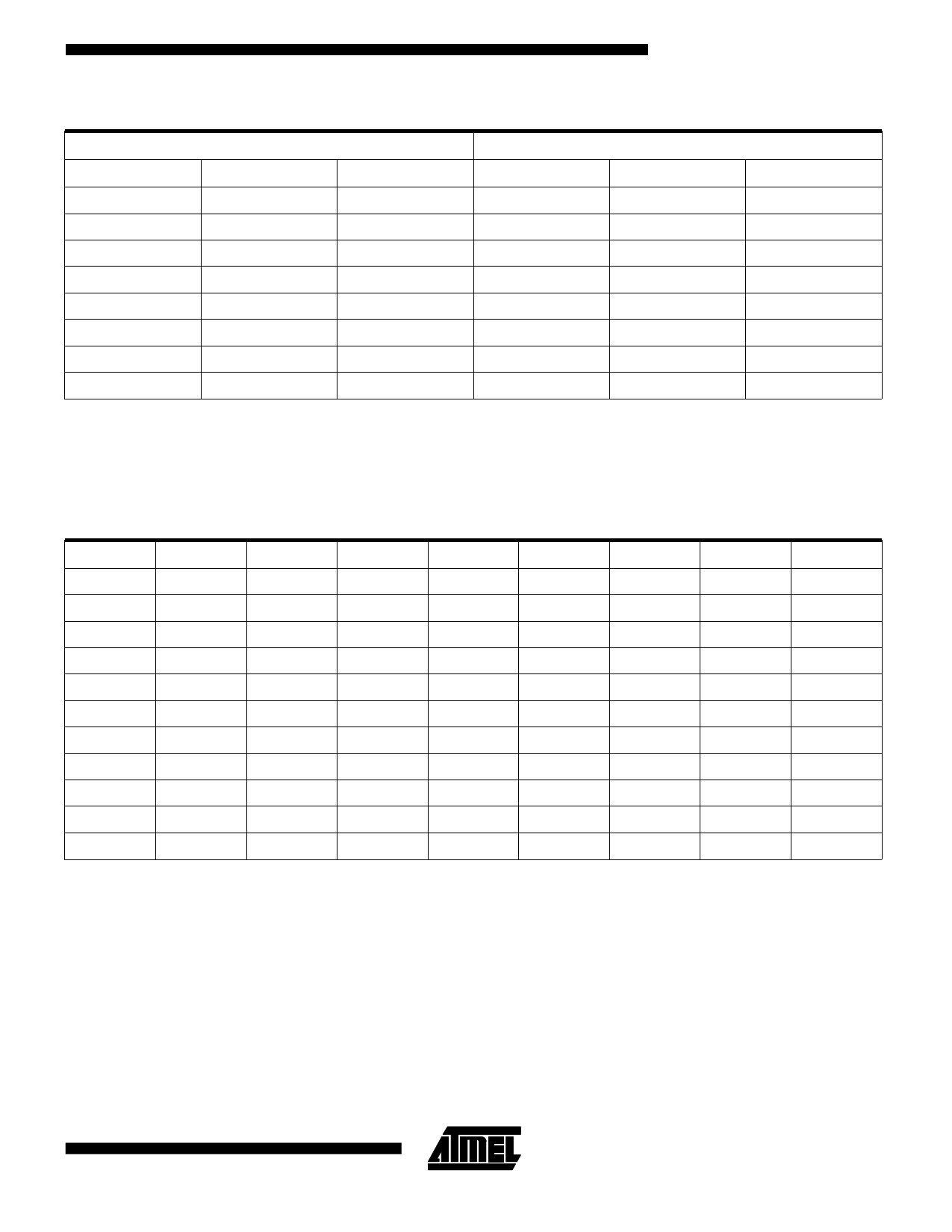
Address Decoder Operation
SGL/DBL* = H
SEL[1:0]
DEC[2:0]
ICE[7:0]*
XX
LLL
HHHHHHHL
XX
LLH
HHHHHHLH
XX
LHL
HHHHHLHH
XX
LHH
HHHHLHHH
XX
HLL
HHHLHHHH
XX
HLH
HHLHHHHH
XX
HHL
HLHHHHHH
XX
HHH
LHHHHHHH
SEL[1:0]
LL
LL
LL
LL
LH
HL
HH
SGL/DBL* = L
DEC[2:0]
XLL
XLH
XHL
XHH
ICE[7:0]*
HHHHHHHL
HHHHHHLH
HHHHHLHH
HHHHLHHH
XXX
XXX
XXX
HHLHHHHH
HLHHHHHH
LHHHHHHH
The AT43101 provides separate output and write enables for
the upper and lower bytes of the memory array to implement
byte addressing. The assertion of these outputs under the
control of A0, CE2*, CE1*, OE* and WE* is given by the
following table when REG* is high.
Byte Control Logic Operation
OE*
WE*
CE2*
CE1*
A0
IOEL*
IOEH*
IWEL*
IWEH*
H
H
X
X
X
H
H
H
H
L
H
H
H
X
H
H
H
H
L
H
H
L
L
L
H
H
H
L
H
H
L
H
H
L
H
H
L
H
L
H
X
H
L
H
H
L
H
L
L
X
L
L
H
H
H
L
H
H
X
H
H
H
H
H
L
H
L
L
H
H
L
H
H
L
H
L
H
H
H
H
L
H
L
L
H
X
H
H
H
L
H
L
L
L
X
H
H
L
L
The IWP* input provides write protection for common
memory. When IWP* is low, assertion of IWEL* and
IWEH* is inhibited. The WPATT input provides write pro-
tection for the attribute memory when high. This signal is
pulled down internally for applications not requiring write
protection. In addition, the AT43101 is disabled for 3 milli-
seconds during power up to prevent writes from occurring
to either attribute or common memory. The state of the
A*/B pin is also latched at this time. The AT43101 does
not support the optional PCMCIA WAIT* signal.
5
Share Link: