AT43101 Ver la hoja de datos (PDF) - Atmel Corporation
Número de pieza
componentes Descripción
Lista de partido
AT43101
Atmel Corporation

AT43101 Datasheet PDF : 14 Pages
| |||
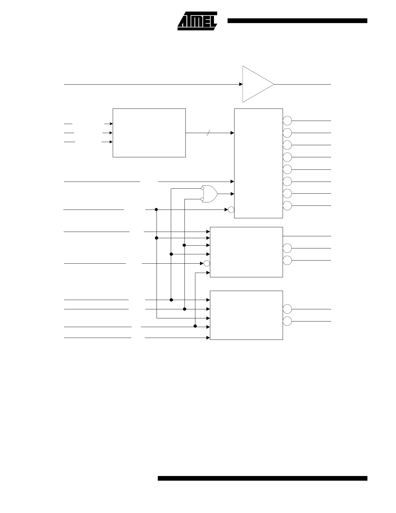
Block Diagram for Mode B Operation
A[24:9]
ADDRESS
BUFFER
IA[24:9]
SGL/DBL*
DEC[2:0]
SEL[1:0]
SGL/DBL* LOGIC
REG*
Reset
WE*
IWP*
3
DEC
ONE OF
EIGHT
DECODER
EN
EN
EN
BYTE WRITE
CONTROL LOGIC
ICE7*
ICE6*
ICE5*
ICE4*
ICE3*
ICE2*
ICE1*
ICE0*
WP
IWEH*
IWEL*
CE1*
CE2*
A0
OE*
BYTE READ
CONTROL LOGIC
IOEH*
IOEL*
The AT43101 supports both Common and Attribute
Memory read and write cycles of word and byte width.
Common memory, the external memory devices on the PC
card, is selected when REG* is high and can be accessed
in either byte or word mode. Attribute memory, the internal
256x8 E2PROM, is selected when REG* is low and can
only be accessed as the even byte of it’s 512 byte address
space. Byte/word addressing is controlled by CE1*, CE2*
and A0. OE* functions as an active low output enable.
WE* functions as an active low write enable.
Memory access functionality is defined by the following
table. When Attribute Memory is selected by the assertion
of REG*, only the lower data bus, D[7:0] is valid and only
even numbered addresses may be accessed. Accord-
ingly, an entry of “H or L” in the REG* of the function table
means the access is supported for both Common Memory
and Attribute Memory. An entry of “H only” means the ac-
cess is supported for Common Memory accesses but not
for Attribute Memory accesses.
During word accesses of Common Memory, D[15:0] and
ID[15:0] are active. During byte accesses (other than Odd
Byte Only accesses), the PCMCIA transfers take place on
D[7:0] and the AT43101 performs the required byte lane
swapping based on A0 to and from D[15:8] or D[7:0]
6
AT43101
Share Link: