NM95MS16 Ver la hoja de datos (PDF) - Fairchild Semiconductor
Número de pieza
componentes Descripción
Lista de partido
NM95MS16 Datasheet PDF : 10 Pages
| |||
INTRODUCTION (Continued)
EEPROM Programming
The entire 6 kbits of EEPROM can be programmed through the
ISA bus. The EEPROM can be programmed by putting the device
(NM95MS16) in the Config. state (as defined in the PnP standard).
Under this state 4 registers at address 0xF0–0xF3 are accessible
to program the EEPROM. The data to be programmed is loaded
in register at address 0xF3 and 0xF2 (LSB and MSB respectively).
The address to be programmed is loaded in register at address
0xF1. The Ninth bit of address for 6 kbits of memory is provided
through the register at address 0xF0. Both read write are possible.
The actual operation does not begin until Go Ahead (GA) bit is set.
Programming a word takes approximately 10 ms. The status of the
operation can be polled by the Status bit. This bit is set when the
operation is in progress and will be reset when complete. The
register at address 0xF0 is COMMAND register. This is the
handshake register in programming the EEPROM and is ex-
plained below in a tabular format.
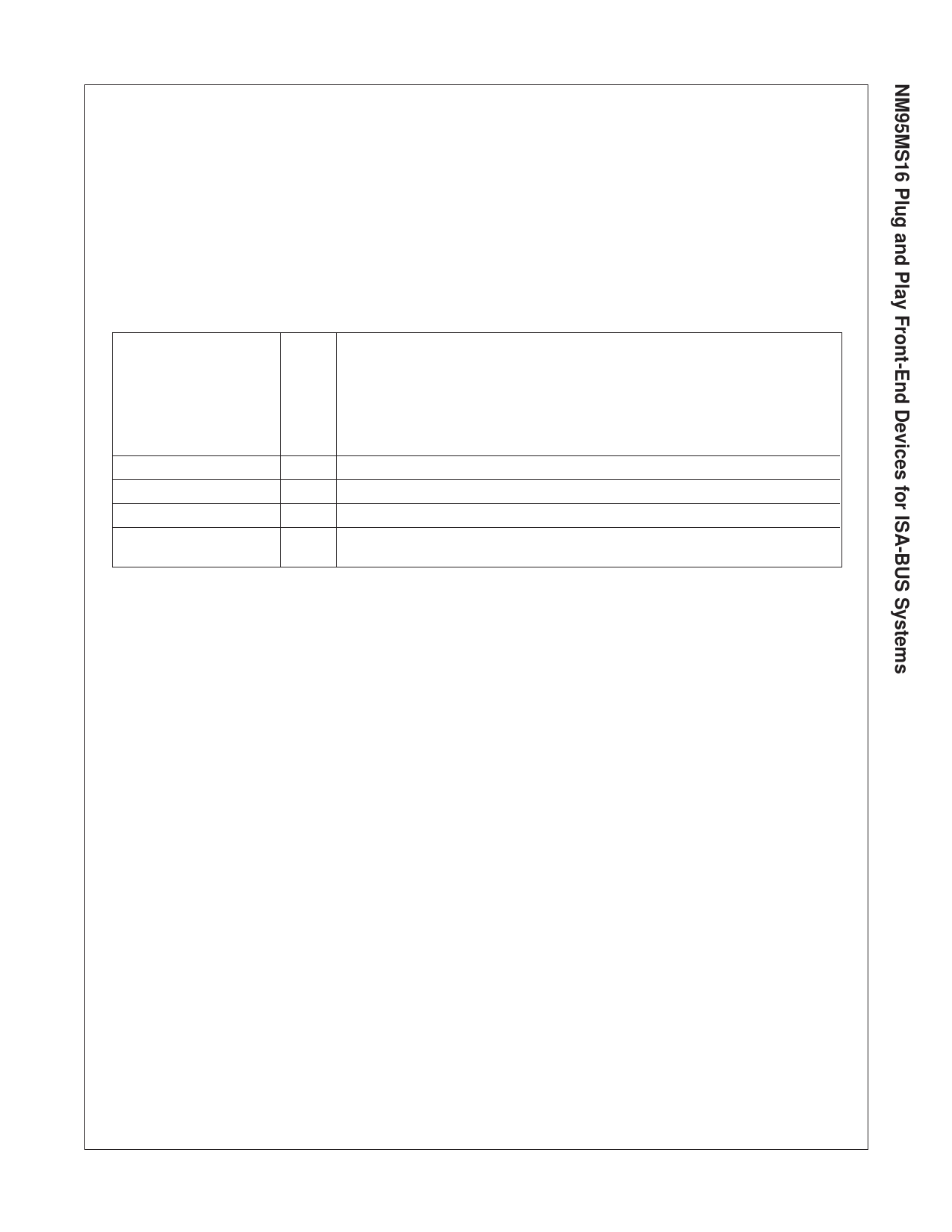
COMMAND Register
Address Register
Data Register
Data Register
STATUS Register
0xF0
0xF1
0xF2
0xF3
0x05
Bit[1:0]
Bit[2]
Bit[6:3]
Bit[7]
—OP Code bits
10 - Read operation
01 - Write operation
11 - Erase operation
—GA(Go ahead bits)
If set to 1 the programming will continue.
—Reserved, should be 0.
—It provides A8 of the address. A[0:7] is provided by 0xF1 reg. (Note 7)
AddressRegister [A0–A7]
Data Byte [MSB]
Data Byte [LSB]
Bit[0]
—Status/Busy bit.
“0” if busy, “1” is done.
Note 7: The PNP resource data portion of the internal memory is at high address. Hence to program that portion, bit [7] of register 0xF0 (Address A8) should be set to “1”.
8
www.fairchildsemi.com
Share Link: 