LTC1412IG Ver la hoja de datos (PDF) - Linear Technology
Número de pieza
componentes Descripción
Lista de partido
LTC1412IG Datasheet PDF : 16 Pages
| |||
LTC1412
APPLICATIONS INFORMATION
SAMPLE
AIN+
SAMPLE
AIN–
CSAMPLE+
HOLD
CSAMPLE–
HOLD
CDAC+
VDAC+
CDAC–
ZEROING SWITCHES
HOLD
HOLD
+
COMP
–
VDAC–
12
SAR
OUTPUT
LATCHES
•••
D11
D0
1412 F01
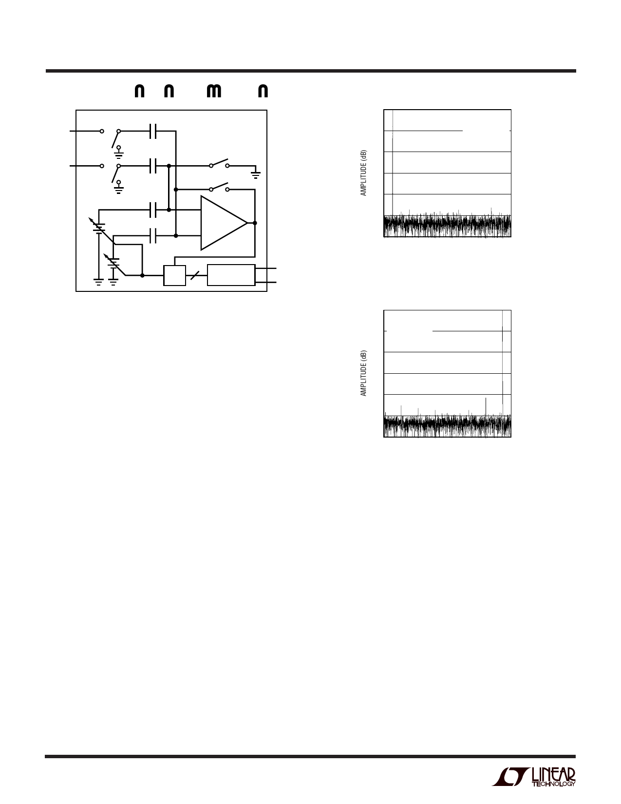
Figure 1. Simplified Block Diagram
sample-and-hold capacitors to acquire the analog signal.
During the convert phase the comparator zeroing switches
open, putting the comparator into compare mode. The
input switches connect the CSAMPLE capacitors to ground,
transferring the differential analog input charge onto the
summing junction. This input charge is successively com-
pared with the binary-weighted charges supplied by the
differential capacitive DAC. Bit decisions are made by the
high speed comparator. At the end of a conversion, the
differential DAC output balances the AIN+ and AIN– input
charges. The SAR contents (a 12-bit data word) which
represents the difference of AIN+ and AIN– are loaded into
the 12-bit output latches.
Dynamic Performance
The LTC1412 has excellent high speed sampling capabil-
ity. FFT (Fast Four Transform) test techniques are used to
test the ADC’s frequency response, distortion and noise at
the rated throughput. By applying a low distortion sine
wave and analyzing the digital output using an FFT algo-
rithm, the ADC’s spectral content can be examined for
frequencies outside the fundamental. Figure 2 shows a
typical LTC1412 FFT plot.
Signal-to-Noise Ratio
The signal-to-noise plus distortion ratio [S/(N + D)] is the
ratio between the RMS amplitude of the fundamental input
frequency to the RMS amplitude of all other frequency
components at the A/D output. The output is band limited
0
fSMPL = 3Msps
fIN = 97.412kHz
– 20
SFDR = 93.3dB
SINAD = 73dB
– 40
– 60
– 80
– 100
– 120
0
200 400 600 800 1000 1200 1400
FREQUENCY (kHz)
1412 F02a
Figure 2a. LTC1412 Nonaveraged, 4096 Point FFT,
Input Frequency = 100kHz
0
fSMPL = 3Msps
fIN = 1.419kHz
–20 SFDR = 83dB
SINAD = 72.5dB
SNR = 73db
– 40
– 60
– 80
– 100
– 120
0
200 400 600 800 1000 1200 1400
FREQUENCY (kHz)
1412 F02B
Figure 2b. LTC1412 Nonaveraged, 4096 Point FFT,
Input Frequency = 1.45MHz
to frequencies from above DC and below half the sampling
frequency. Figure 2 shows a typical spectral content with
a 3MHz sampling rate and a 100kHz input. The dynamic
performance is excellent for input frequencies up to and
beyond the Nyquist limit of 1.5MHz.
Effective Number of Bits
The Effective Number of Bits (ENOBs) is a measurement of
the resolution of an ADC and is directly related to the
S/(N + D) by the equation:
N = [S/(N + D) – 1.76]/6.02
where N is the effective number of bits of resolution and
S/(N + D) is expressed in dB. At the maximum sampling
rate of 3MHz the LTC1412 maintains near ideal ENOBs up
to the Nyquist input frequency of 1.5MHz. Refer to
Figure␣ 3.
8
Share Link: 