HI3-DAC80V-5 Ver la hoja de datos (PDF) - Intersil
Número de pieza
componentes Descripción
Lista de partido
HI3-DAC80V-5 Datasheet PDF : 7 Pages
| |||
HI-DAC80V, HI-DAC85V
Thermal Drift
Thermal drift is based on measurements at 25oC, at high
f(oTrHt)haenhdiglohw(T(THL-)2t5eomCp)earantdurleosw.
Drift calculations are made
(25oC-TL) ranges, and the
larger of the two values is given as a specification represent-
ing worst case drift.
Gain Drift, Offset Drift, Reference Drift and Total Bipolar Drift
are calculated in parts per million per oC as follows:
GainDrift = ∆-----F----S-F---R-S-----R⁄---∆----°---C-- × 106
values within the specified operating range. Gain and offset
errors must be calibrated to zero at 25oC. Then the specified
limits for Total Error apply for any input code and for any
temperature within the specified operating range.
Power Supply Sensitivity
Power Supply Sensitivity is a measure of the change in gain
and offset of the D/A converter resulting from a change in
-VS, or +VS supplies. It is specified under DC conditions and
expressed as full scale range percent of change divided by
power supply percent change.
OffsetDrift = ∆-----O-----f--f-F-s---S-e---t-R---⁄--∆----°---C--- × 106
ReferenceDrift = ∆----V-----R----VE----RF----E-⁄--(-F--∆----°---C-----) × 106
To talBipolarDrift = ∆----V-----O-F-----⁄S--(--R∆-----°--C------) × 106
NOTE: FSR = Full Scale Output Voltage - Zero Scale Output
Voltage
o∆rFFSSRR=(F25SoRC()T-HF)S-RFS(TRL)(.25oC),
VO = Steady State response to any input code.
Total Bipolar Drift is the variation of output voltage with
temperature, in the bipolar mode of operation. It represents
the net effect of drift in Gain, Offset, Linearity and Reference
Voltage. Total Bipolar Drift values are calculated, based on
measurements as explained above. Gain and Offset need
not be calibrated to zero at 25oC. The specified limits for
TBD apply for any input code and for any power supply set-
ting within the specified operating range.
Accuracy
PSS = -∆---------F------u--------l--Fl----S----SV-------c---∆---R-S----a---V-----(--(--l--N---e-SN---------o-R----o-×---m------a-m----1----i---n--n-0---i------nga0---------l-a-e---)-----l--×--)--------1-------0-------0----
Glitch
A glitch on the output of a D/A converter is a transient spike
resulting from unequal internal ON-OFF switching times.
Worst case glitches usually occur at half-scale, i.e., the
major carry code transition from 011...1 to 100...0 or vice
versa. For example, if turn ON is greater than OFF for
011...1 to 100...0, an intermediate state of 000...0 exists,
such that, the output momentarily glitches toward zero out-
put. Matched switching times and fast switching will reduce
glitches considerably. (Measured as one half the Product of
duration and amplitude.)
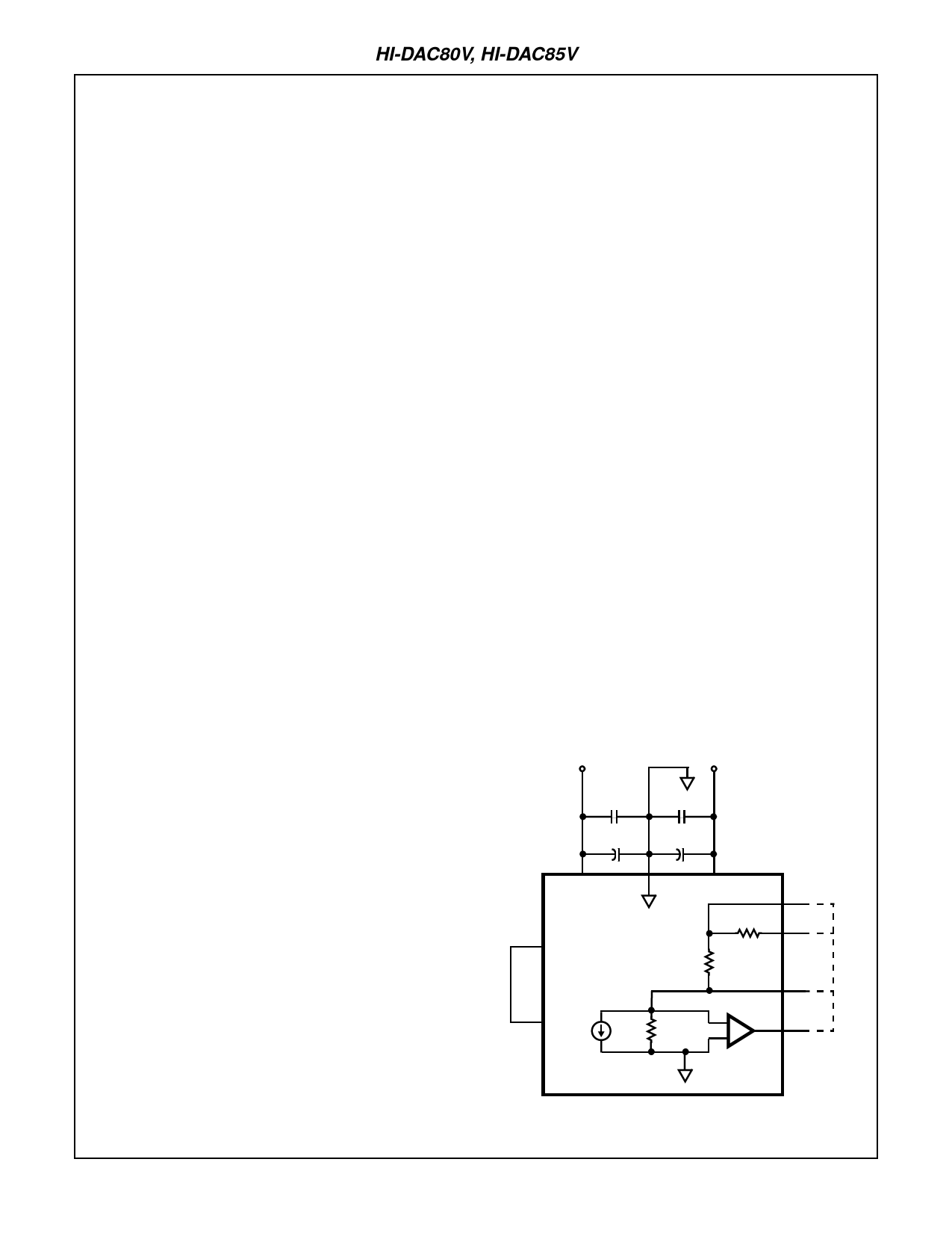
Decoupling and Grounding
For best accuracy and high frequency performance, the
grounding and decoupling scheme shown in Figure 1 should
be used. Decoupling capacitors should be connected close
to the HI-DAC80V/HI-DAC85V (preferably to the device pins)
and should be tantalum or electrolytic bypassed with
ceramic types for best high frequency noise rejection.
Linearity Error (Short for “Integral Linearity Error.” Also,
sometimes called “Integral Nonlinearity” and “Nonlinearity”.)
The maximum deviation of the actual transfer characteristic
from an ideal straight line. The ideal line is positioned
according to end-point linearity for D/A converter products
from Intersil Corporation , i.e., the line is drawn between the
end-points of the actual transfer characteristic (codes 00...0
and 11...1).
Differential Linearity Error The difference between one
LSB and the output voltage change corresponding to any
two consecutive codes. A Differential Nonlinearity of ±1 LSB
or less guarantees monotonicity.
Monotonicity The property of a D/A converter’s transfer
function which guarantees that the output derivative will not
change sign in response to a sequence of increasing (or
decreasing) input codes. That is, the only output response to
a code change is to remain constant, increase for Increasing
code, or decrease for decreasing code.
-VS
0.01µF
1µF
+VS
0.01µF
1µF
14
24
16
21
22
18
19
20
-
15
+
Total Error The net output error resulting from all internal
effects (primarily non-ideal Gain, Offset, Linearity and
Reference Voltage). Supply voltages may be set to any
FIGURE 1.
10-1038
Share Link: 