XR16C864 Ver la hoja de datos (PDF) - Exar Corporation
Número de pieza
componentes Descripción
Lista de partido
XR16C864 Datasheet PDF : 51 Pages
| |||
REV. 2.2.0
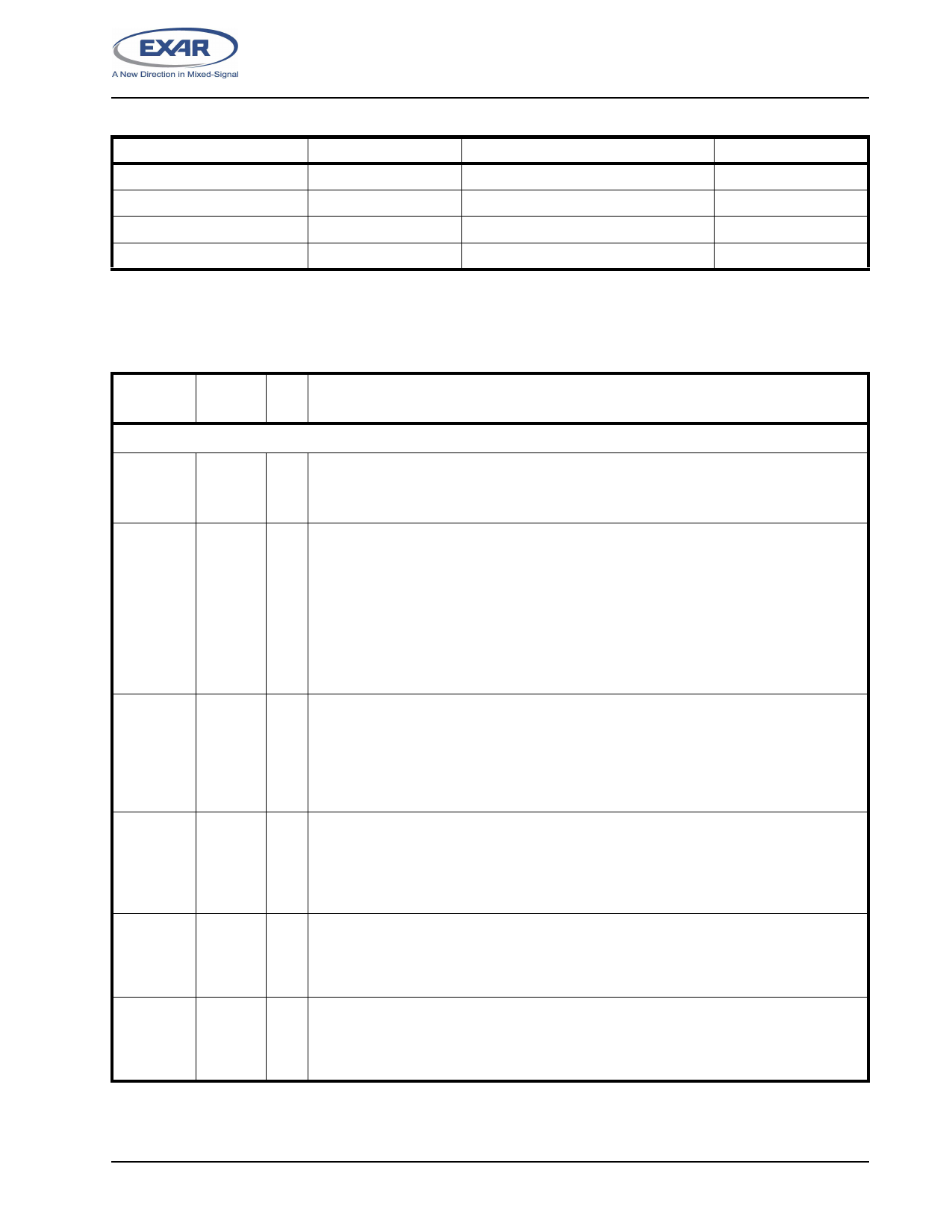
ORDERING INFORMATION
PART NUMBER
XR16C864CQ-F
XR16C864CQTR-F
XR16C864IQ-F
XR16C864IQTR-F
PACKAGE
100-Lead QFP
100-Lead QFP
100-Lead QFP
100-Lead QFP
XR16C864
2.97V TO 5.5V QUAD UART WITH 128-BYTE FIFO
OPERATING TEMPERATURE RANGE
0°C to +70°C
0°C to +70°C
-40°C to +85°C
-40°C to +85°C
DEVICE STATUS
Active
Active
Active
Active
NOTE: TR = Tape and Reel, -F = Green / RoHS
PIN DESCRIPTIONS
Pin Description
NAME
100-QFP
TYPE
PIN #
DESCRIPTION
DATA BUS INTERFACE
A2
37
I Address data lines [2:0]. These 3 address lines select one of the internal registers in
A1
38
UART channels A-D during a data bus transaction.
A0
39
D7
95
I/O Data bus lines [7:0] (bidirectional).
D6
94
D5
93
D4
92
D3
91
D2
90
D1
89
D0
88
IOR#
(N.C.)
66
I When 16/68# pin is at logic 1, the Intel bus interface is selected and this input becomes
read strobe (active low). The falling edge instigates an internal read cycle and retrieves
the data byte from an internal register pointed by the address lines [A2:A0], puts the data
byte on the data bus to allow the host processor to read it on the rising edge.
When 16/68# pin is at logic 0, the Motorola bus interface is selected and this input is not
used.
IOW#
15
I When 16/68# pin is at logic 1, it selects Intel bus interface and this input becomes write
(R/W#)
strobe (active low). The falling edge instigates the internal write cycle and the rising edge
transfers the data byte on the data bus to an internal register pointed by the address lines.
When 16/68# pin is at logic 0, the Motorola bus interface is selected and this input
becomes read (logic 1) and write (logic 0) signal.
CSA#
(CS#)
13
I When 16/68# pin is at logic 1, this input is chip select A (active low) to enable channel A in
the device.
When 16/68# pin is at logic 0, this input becomes the chip select (active low) for the
Motorola bus interface.
CSB#
(A3)
17
I When 16/68# pin is at logic 1, this input is chip select B (active low) to enable channel B in
the device.
When 16/68# pin is at logic 0, this input becomes address line A3 which is used for chan-
nel selection in the Motorola bus interface.
3
Share Link: 