RF2713 Ver la hoja de datos (PDF) - RF Micro Devices
Número de pieza
componentes Descripción
Lista de partido
RF2713 Datasheet PDF : 16 Pages
| |||
RF2713
Pin Function Description (Modulator Configuration)
Interface Schematic
1
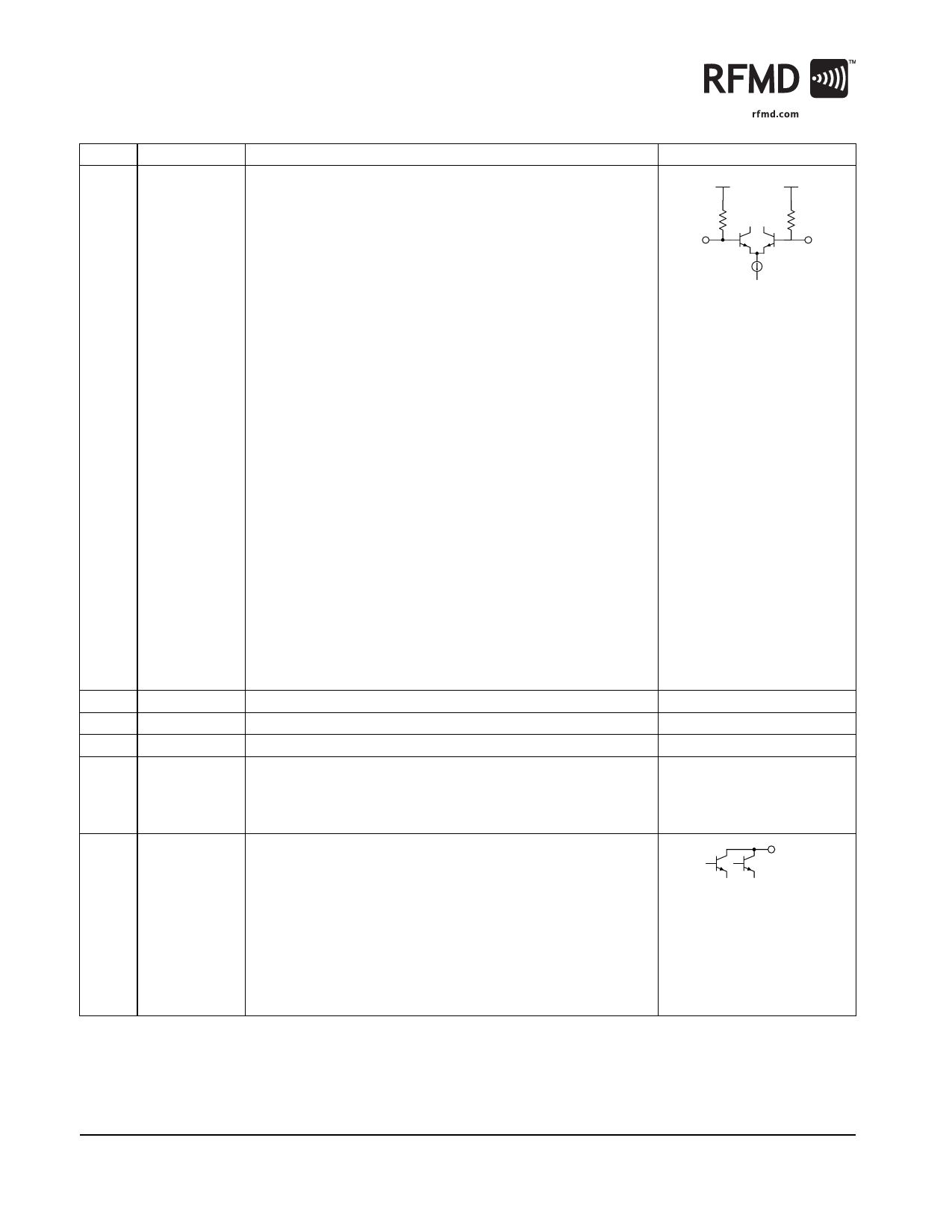
I INPUT A When the RF2713 is configured as a Quadrature Modulator, each mixer is
driven by an independent baseband modulation channel (I and Q). The
VCC
VCC
mixers can be driven single-endedly (as shown in the modulator applica-
tion circuit) or differentially. When driving single-endedly, the B Inputs (pins
1260 Ω
1260 Ω
2 and 4) should be connected to each other. This ensures that the base- INPUT A
band signals will reach each mixer with the same DC reference, yielding
INPUT B
the best carrier suppression. Note that the input impedance changes
according to the drive mode (see the mixer equivalent circuit on the previ-
ous page). The single-ended input impedance (as shown in the modulator
application circuit) is 1200Ω for each of the two inputs. In the balanced
configuration, the input impedance would be 2400Ω for each of the two
inputs.
The mixers are Gilbert Cell designs with balanced inputs. The equivalent
schematic for one of the mixers is shown on the previous page. The input
impedance of each pin is determined by the 1200Ω resistor to VCC in par-
allel with a transistor base. Note from the schematic that all four input pins
have an internally set DC bias. For this reason, all four inputs (pins 1
through 4) should be DC blocked. The capacitance values of the blocking
capacitors is determined by the baseband frequency. When driving sin-
gle-endedly, both the series (pins 1 and 3) and shunt (pins 2 and 4) block-
ing capacitors should be low impedances, relative to the input impedance.
DC bias voltages may be supplied to the inputs pins, if required, in order to
increase the amount of carrier suppression. For example, the DC levels on
the reference inputs (pins 2 and 4) may be offset from each other by add-
ing different resistor values to ground. These resistors should be larger
than 2kΩ. Note from the mixer schematic that all four input pins have an
internally set DC bias. If DC bias is to be supplied, the allowable ranges are
limited. For 5V applications, the DC reference on both I pins or both Q pins
must not go below 2.7VDC, and in no case should the DC voltage on any of
the four pins go below 2.0VDC or above 5.5VDC. IF a DC reference is to be
supplied, the source must also be capable of sinking current. If optimizing
carrier suppression further is not a concern, it is recommended that all
four inputs (pins 1 through 4) be DC blocked.
2
I INPUT B Same as pin 1, except complementary input.
See pin 1.
3
Q INPUT A Same as pin 1, except Q Buffer Amplifier.
See pin 1.
4
Q INPUT B Same as pin 3, except complementary input.
See pin 1.
5
BG OUT
Band Gap voltage reference output. This voltage output is held constant
over variations in supply voltage and operating temperature and may be
used as a reference for other external circuitry. This pin should not be
loaded such that the sourced current exceeds 1mA. This pin should be
bypassed with a large (0.1μF) capacitor.
6
I IF OUT
Connecting pins 6 and 7 to each other accomplishes the summing function
of the upconverted I and Q channels. In addition, because these outputs
are open collector type, they must be connected to VCC in order to properly
bias the Gilbert Cell mixers. Maximum gain and output power occur when
the load on these two pins is ~1200Ω. In most applications the impedance
of the next stage will be lower and a reactive impedance transforming
match should be used if maximum gain and output level are of concern.
For applications where the gain is not as critical, a 1200Ω resistor may be
added in parallel with a choke inductor. If neither gain nor output level is
critical, the inductor may be replaced with a resistor that sets the desired
source impedance to drive the next stage. If the next stage is an "open" at
DC, the blocking capacitor may be eliminated.
IF OUT
6 of 16
7628 Thorndike Road, Greensboro, NC 27409-9421 · For sales or technical
support, contact RFMD at (+1) 336-678-5570 or sales-support@rfmd.com.
Rev A5 DS061016
Share Link: 